
Increased fracture depth range in controlled spalling of (100)-oriented germanium via electroplating
Abstract
Controlled spalling in (100)-oriented germanium using a nickel stressor layer shows promise for semiconductor device exfoliation and kerfless wafering. Demonstrated spall depths of 7-60 um using DC sputtering to deposit the stressor layer are appropriate for the latter application but spall depths < 5 um may be required to minimize waste for device applications. This work investigates the effect of tuning both electroplating current density and electrolyte chemistry on the residual stress in the nickel and on the achievable spall depth range for the Ni/Ge system as a lower-cost, higher-throughput alternative to sputtering. By tuning current density and electrolyte phosphorous concentration, it is shown that electroplating can successfully span the same range of spalled thicknesses as has previously been demonstrated by sputtering and can reach sufficiently high stresses to enter a regime of thickness (<7 um) appropriate to minimize substrate consumption for device applications.
- Authors:
-
- Colorado School of Mines, Golden, CO (United States)
- National Renewable Energy Lab. (NREL), Golden, CO (United States)
- Colorado School of Mines, Golden, CO (United States); National Renewable Energy Lab. (NREL), Golden, CO (United States)
- Publication Date:
- Research Org.:
- National Renewable Energy Lab. (NREL), Golden, CO (United States)
- Sponsoring Org.:
- USDOE Office of Energy Efficiency and Renewable Energy (EERE), Renewable Power Office. Solar Energy Technologies Office
- OSTI Identifier:
- 1424582
- Alternate Identifier(s):
- OSTI ID: 1548764
- Report Number(s):
- NREL/JA-5J00-71046
Journal ID: ISSN 0040-6090
- Grant/Contract Number:
- AC36-08GO28308
- Resource Type:
- Accepted Manuscript
- Journal Name:
- Thin Solid Films
- Additional Journal Information:
- Journal Volume: 649; Journal Issue: C; Journal ID: ISSN 0040-6090
- Publisher:
- Elsevier
- Country of Publication:
- United States
- Language:
- English
- Subject:
- 14 SOLAR ENERGY; 36 MATERIALS SCIENCE; flexible electronics; thin film; substrate reuse; germanium; fracture; spalling; layer transfer; exfoliation
Citation Formats
                    Crouse, Dustin, Simon, John, Schulte, Kevin L., Young, David L., Ptak, Aaron J., and Packard, Corinne E. Increased fracture depth range in controlled spalling of (100)-oriented germanium via electroplating.  United States: N. p., 2018.
Web.  doi:10.1016/j.tsf.2018.01.031.
Crouse, Dustin, Simon, John, Schulte, Kevin L., Young, David L., Ptak, Aaron J., & Packard, Corinne E. Increased fracture depth range in controlled spalling of (100)-oriented germanium via electroplating. United States. https://doi.org/10.1016/j.tsf.2018.01.031
                    Crouse, Dustin, Simon, John, Schulte, Kevin L., Young, David L., Ptak, Aaron J., and Packard, Corinne E. Wed .
"Increased fracture depth range in controlled spalling of (100)-oriented germanium via electroplating".  United States.  https://doi.org/10.1016/j.tsf.2018.01.031.  https://www.osti.gov/servlets/purl/1424582.
@article{osti_1424582,

  title        = {Increased fracture depth range in controlled spalling of (100)-oriented germanium via electroplating},

  author       = {Crouse, Dustin and Simon, John and Schulte, Kevin L. and Young, David L. and Ptak, Aaron J. and Packard, Corinne E.},

  abstractNote = {Controlled spalling in (100)-oriented germanium using a nickel stressor layer shows promise for semiconductor device exfoliation and kerfless wafering. Demonstrated spall depths of 7-60 um using DC sputtering to deposit the stressor layer are appropriate for the latter application but spall depths < 5 um may be required to minimize waste for device applications. This work investigates the effect of tuning both electroplating current density and electrolyte chemistry on the residual stress in the nickel and on the achievable spall depth range for the Ni/Ge system as a lower-cost, higher-throughput alternative to sputtering. By tuning current density and electrolyte phosphorous concentration, it is shown that electroplating can successfully span the same range of spalled thicknesses as has previously been demonstrated by sputtering and can reach sufficiently high stresses to enter a regime of thickness (<7 um) appropriate to minimize substrate consumption for device applications.},

  doi          = {10.1016/j.tsf.2018.01.031},

  journal      = {Thin Solid Films},

  number       = C,

  volume       = 649,

  place        = {United States},

  year         = {Wed Jan 31 00:00:00 EST 2018},

  month        = {Wed Jan 31 00:00:00 EST 2018}

}
 Search WorldCat to find libraries that may hold this journal
Web of Science
Figures / Tables:
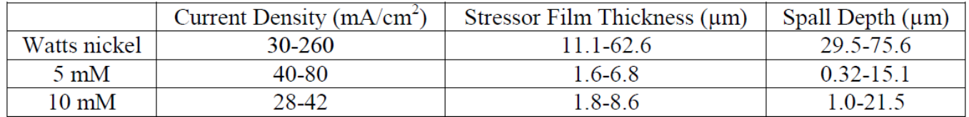 Table 1: Measured Ni film thicknesses and Ge spall depth for controllably spalled samples for different electrolyte chemistries
Works referenced in this record:
Techno-economic analysis of three different substrate removal and reuse strategies for III-V solar cells: Techno-economic analysis for III-V solar cells
journal, May 2016
- Ward, J. Scott; Remo, Timothy; Horowitz, Kelsey
- Progress in Photovoltaics: Research and Applications, Vol. 24, Issue 9
26.1% thin-film GaAs solar cell using epitaxial lift-off
journal, September 2009
- Bauhuis, G. J.; Mulder, P.; Haverkamp, E. J.
- Solar Energy Materials and Solar Cells, Vol. 93, Issue 9
Kerf-Less Removal of Si, Ge, and III–V Layers by Controlled Spalling to Enable Low-Cost PV Technologies
journal, April 2012
- Bedell, Stephen W.; Shahrjerdi, Davood; Hekmatshoar, Bahman
- IEEE Journal of Photovoltaics, Vol. 2, Issue 2
Layer transfer by controlled spalling
journal, March 2013
- Bedell, Stephen W.; Fogel, Keith; Lauro, Paul
- Journal of Physics D: Applied Physics, Vol. 46, Issue 15
Ultralight High-Efficiency Flexible InGaP/(In)GaAs Tandem Solar Cells on Plastic
journal, December 2012
- Shahrjerdi, Davood; Bedell, Stephen W.; Bayram, Can
- Advanced Energy Materials, Vol. 3, Issue 5
Energy band engineering of flexible gallium arsenide through substrate cracking with pre-tensioned films
journal, July 2016
- Alharbi, Abdullah; Shahrjerdi, Davood
- physica status solidi (RRL) - Rapid Research Letters, Vol. 10, Issue 8
Mixed Mode Cracking in Layered Materials
book, January 1991
- Hutchinson, J. W.; Suo, Z.
- Advances in Applied Mechanics, Vol. 29, p. 63-191
The cracking and decohesion of thin films
journal, October 1988
- Evans, A. G.; Drory, M. D.; Hu, M. S.
- Journal of Materials Research, Vol. 3, Issue 5
Controlled exfoliation of (100) GaAs-based devices by spalling fracture
journal, January 2016
- Sweet, Cassi A.; Schulte, Kevin L.; Simon, John D.
- Applied Physics Letters, Vol. 108, Issue 1
Effects of Process Conditions on Properties of Electroplated Ni Thin Films for Microsystem Applications
journal, January 2006
- Luo, J. K.; Pritschow, M.; Flewitt, A. J.
- Journal of The Electrochemical Society, Vol. 153, Issue 10
An improved technique for determining hardness and elastic modulus using load and displacement sensing indentation experiments
journal, June 1992
- Oliver, W. C.; Pharr, G. M.
- Journal of Materials Research, Vol. 7, Issue 06, p. 1564-1583
Celebrating the 100th anniversary of the Stoney equation for film stress: Developments from polycrystalline steel strips to single crystal silicon wafers
journal, January 2009
- Janssen, G. C. A. M.; Abdalla, M. M.; van Keulen, F.
- Thin Solid Films, Vol. 517, Issue 6
Tailoring and patterning the grain size of nanocrystalline alloys
journal, January 2007
- Detor, A.; Schuh, C.
- Acta Materialia, Vol. 55, Issue 1
Structural transitions in electroplated Ni-P alloys
journal, July 1989
- McMahon, G.; Erb, U.
- Journal of Materials Science Letters, Vol. 8, Issue 7
Electrochemical nickel–phosphorus alloy formation
journal, October 2003
- Daly, B. P.; Barry, F. J.
- International Materials Reviews, Vol. 48, Issue 5
Dislocation strengthening in FCC metals and in BCC metals at high temperatures
journal, March 2017
- Madec, Ronan; Kubin, Ladislas P.
- Acta Materialia, Vol. 126
Anisotropy effects on the reliability of single-crystal silicon
journal, November 2010
- Borrero-López, Oscar; Vodenitcharova, Tania; Hoffman, Mark
- Scripta Materialia, Vol. 63, Issue 10
Sub-5 μ m-thick spalled single crystal Si foils by decoupling crack initiation and propagation
journal, September 2016
- Lee, Yong Hwan; Kim, Yong-Jae; Han, Seung Min Jane
- Applied Physics Letters, Vol. 109, Issue 13
Fracture toughness of germanium determined with the Vickers indentation technique
journal, August 1988
- Lemaitre, P.
- Journal of Materials Science Letters, Vol. 7, Issue 8
Works referencing / citing this record:
Microstructural characterization and film-forming mechanism of a phosphate chemical conversion ceramic coating prepared on the surface of 2A12 aluminum alloy
journal, January 2019
- Huang, Shuai; Wang, Jian; Wei, Xiaowei
- RSC Advances, Vol. 9, Issue 33
Figures / Tables found in this record: