Graphene-Insulator-Semiconductor Junction for Hybrid Photodetection Modalities
- Sandia National Lab. (SNL-NM), Albuquerque, NM (United States); DOE/OSTI
- Sandia National Lab. (SNL-NM), Albuquerque, NM (United States)
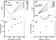
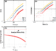
A sensitive optical detector is presented based on a deeply depleted graphene-insulator-semiconducting (D2GIS) junction, which offers the possibility of simultaneously leveraging the advantages of both charge integration and localized amplification. Direct read-out and built-in amplification are accomplished via photogating of a graphene field-effect transistor (GFET) by carriers generated within a deeply depleted low-doped silicon substrate. Analogous to a depleted metal-oxide-semiconducting junction, photo-generated charge collects in the potential well that forms at the semiconductor/insulator interface and induces charges of opposite polarity within the graphene film modifying its conductivity. This device enables simultaneous photo-induced charge integration with continuous “on detector” readout through use of graphene. The resulting devices exhibit responsivities as high as 2,500 A/W (25,000 S/W) for visible wavelengths and a dynamic range of 30 dB. As both the graphene and device principles are transferrable to arbitrary semiconductor absorbers, D2GIS devices offer a high-performance paradigm for imaging across the electromagnetic spectrum
- Research Organization:
- Sandia National Laboratories (SNL-NM), Albuquerque, NM (United States). Center for Integrated Nanotechnologies (CINT) )
- Sponsoring Organization:
- USDOE National Nuclear Security Administration (NNSA); USDOE Laboratory Directed Research and Development (LDRD) Program
- Grant/Contract Number:
- NA0003525
- OSTI ID:
- 1624359
- Journal Information:
- Scientific Reports, Journal Name: Scientific Reports Journal Issue: 1 Vol. 7; ISSN 2045-2322
- Publisher:
- Nature Publishing GroupCopyright Statement
- Country of Publication:
- United States
- Language:
- English
Tunable dual-band graphene-based infrared reflectance filter
|
journal | January 2018 |


Similar Records
Interface Defect Engineering for Improved Graphene-Oxide-Semiconductor Junction Photodetectors