Tunable and laser-reconfigurable 2D heterocrystals obtained by epitaxial stacking of crystallographically incommensurate Bi2Se3 and MoS2 atomic layers
- Northeastern Univ., Boston, MA (United States)
- Northeastern Univ., Boston, MA (United States); Los Alamos National Lab. (LANL), Los Alamos, NM (United States)
- Northeastern Univ., Boston, MA (United States); Univ. of Electronic Science and Technology of China, Sichuan (People's Republic of China)
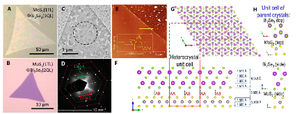
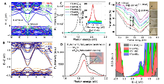
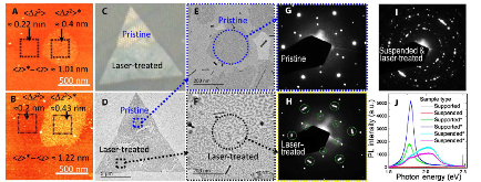
Vertical stacking is widely viewed as a promising approach for designing advanced functionalities using two-dimensional (2D) materials. Combining crystallographically commensurate materials in these 2D stacks has been shown to result in rich new electronic structure, magnetotransport, and optical properties. In this context, vertical stacks of crystallographically incommensurate 2D materials with well-defined crystallographic order are a counterintuitive concept and, hence, fundamentally intriguing. We show that crystallographically dissimilar and incommensurate atomically thin MoS2 and Bi2Se3 layers can form rotationally aligned stacks with long-range crystallographic order. Our first-principles theoretical modeling predicts heterocrystal electronic band structures, which are quite distinct from those of the parent crystals, characterized with an indirect bandgap. Experiments reveal striking optical changes when Bi2Se3 is stacked layer by layer on monolayer MoS2, including 100% photoluminescence (PL) suppression, tunable transmittance edge (1.1→0.75 eV), suppressed Raman, and wide-band evolution of spectral transmittance. Disrupting the interface using a focused laser results in a marked the reversal of PL, Raman, and transmittance, demonstrating for the first time that in situ manipulation of interfaces can enable “reconfigurable” 2D materials. We demonstrate submicrometer resolution, “laser-drawing” and “bit-writing,” and novel laser-induced broadband light emission in these heterocrystal sheets.
- Research Organization:
- Energy Frontier Research Centers (EFRC), Washington, D.C. (United States). Center for the Computational Design of Functional Layered Materials (CCDM); Lawrence Berkeley National Laboratory (LBNL), Berkeley, CA (United States). National Energy Research Scientific Computing Center
- Sponsoring Organization:
- USDOE Office of Science (SC), Basic Energy Sciences (BES) (SC-22)
- Grant/Contract Number:
- AC02-05CH11231; FG02-07ER46352; SC0012575
- OSTI ID:
- 1469909
- Journal Information:
- Science Advances, Journal Name: Science Advances Journal Issue: 7 Vol. 3; ISSN 2375-2548
- Publisher:
- AAASCopyright Statement
- Country of Publication:
- United States
- Language:
- English


Similar Records
Tunable and reconfigurable atomically thin heterostructures
Oxygen-Induced In Situ Manipulation of the Interlayer Coupling and Exciton Recombination in Bi2Se3/MoS2 2D Heterostructures
Patent
·
Tue Apr 05 00:00:00 EDT 2022
·
OSTI ID:1892792
Oxygen-Induced In Situ Manipulation of the Interlayer Coupling and Exciton Recombination in Bi2Se3/MoS2 2D Heterostructures
Journal Article
·
Sun Apr 07 20:00:00 EDT 2019
· ACS Applied Materials and Interfaces
·
OSTI ID:1527368