Large-Area Subwavelength Aperture Arrays Fabricated Using Nanoimprint Lithography
- Berkeley Sensor and Actuator Center, Berkeley, CA (United States); Univ. of California, Davis, CA (United States). Department of Mechanical and Aeronautical Engineering; Sandia National Lab. (SNL-CA), Livermore, CA (United States)
- Sandia National Lab. (SNL-CA), Livermore, CA (United States); Xradia, Inc., Concord, CA (United States)
- Sandia National Lab. (SNL-CA), Livermore, CA (United States)
- Stanford Univ., CA (United States). Department of Electrical Engineering
- Berkeley Sensor and Actuator Center, Berkeley, CA (United States); Univ. of California, Davis, CA (United States). Department of Mechanical and Aeronautical Engineering
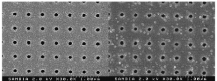
In this paper, we report on the fabrication and characterization of large-area 2-D square arrays of subwavelength holes in Ag and Al films. Fabrication is based on thermal nanoimprint lithography and metal evaporation, without the need for etching, and is compatible with low-cost, large-scale production. Reflectance spectra for these arrays display an intensity minimum whose amplitude, center wavelength, and line width depend on the geometry of the array and the reflectivity of the metal film. By placing various fluids in contact with the subwavelength aperture arrays, we observe that the center wavelength of the reflectance minimum varies linearly with the refractive index of the fluid with a sensitivity of over 500 nm per refractive index unit. Lastly, the surface plasmon theory is used to predict sensitivities to refractive index change with accuracies better than 0.5%.
- Research Organization:
- Sandia National Lab. (SNL-CA), Livermore, CA (United States)
- Sponsoring Organization:
- USDOE National Nuclear Security Administration (NNSA); USDOE Office of Science (SC), Basic Energy Sciences (BES)
- Grant/Contract Number:
- AC04-94AL85000
- OSTI ID:
- 1426959
- Report Number(s):
- SAND-2007-1398J; 526793
- Journal Information:
- IEEE Transactions on Nanotechnology, Vol. 7, Issue 5; ISSN 1536-125X
- Publisher:
- IEEECopyright Statement
- Country of Publication:
- United States
- Language:
- English
Dual Sensing Arrays for Surface Plasmon Resonance (SPR) and Surface-Enhanced Raman Scattering (SERS) Based on Nanowire/Nanorod Hybrid Nanostructures
|
journal | September 2018 |
Highly Sensitive Aluminum-Based Biosensors using Tailorable Fano Resonances in Capped Nanostructures
|
journal | March 2017 |
Plasmonic components fabrication via nanoimprint
|
journal | September 2009 |


Similar Records
Fabrication of subwavelength, binary, antireflection surface-relief structures in the near infrared
Optical Response of Oriented and Highly Anisotropic Subwavelength Metallic Nanostructure Arrays