Morphological Control of GaN and Its Effect within Electrochemical Heterojunctions
- Stanford Univ., Stanford, CA (United States)
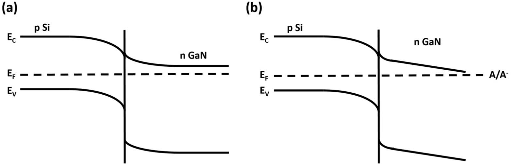
With morphological control through a solid source chemical vapor deposition process, GaN polycrystalline films, single-crystal nanowires, and mixed film/wires are grown on silicon to form a heterojunction that is a basis for III-V nitride device development. By contacting the GaN/Si structure to the CoCp20/ + redox pair and performing impedance spectroscopy measurements, the band diagram of this junction is built for these three configurations. This serves as a basis for understanding the electrical nature of III-V nitride/Si interfaces that exist in several photonic device technologies, especially in context of using GaN nanomaterials grown on silicon for various applications. When these junctions are exposed to low-power UV illumination in contact with the Fc/Fc+ redox pair, photocurrents of 18, 110, and 482 nA/cm2 are generated for the nanowires, mixed film/wires, and films respectively. These currents, along with the electrostatics investigated through the impedance spectroscopy, show the trends of photoconversion with GaN morphology in this junction. Furthermore, they suggest that the mixed film/wires are a promising design for solar-based applications such as photovoltaics and water splitting electrodes.
- Research Organization:
- Energy Frontier Research Centers (EFRC) (United States). Center on Nanostructuring for Efficient Energy Conversion (CNEEC)
- Sponsoring Organization:
- USDOE Office of Science (SC), Basic Energy Sciences (BES)
- Grant/Contract Number:
- SC0001060
- OSTI ID:
- 1397196
- Journal Information:
- Journal of the Electrochemical Society, Vol. 163, Issue 10; Related Information: CNEEC partners with Stanford University (lead); Carnegie Institution at Stanford; Technical University of Denmark; ISSN 0013-4651
- Publisher:
- The Electrochemical SocietyCopyright Statement
- Country of Publication:
- United States
- Language:
- English
Web of Science


Similar Records
Characterization of GaN nanowires grown on PSi, PZnO and PGaN on Si (111) substrates by thermal evaporation
Growth, nitrogen vacancy reduction and solid solution formation in cubic GaN thin films and the subsequent fabrication of superlattice structures using AlN and inn. Final report, 1 June 1986-31 December 1992