Nanoimaging of Electronic Heterogeneity in Bi2Se3 and Sb2Te3 Nanocrystals
- Chinese Academy of Sciences (CAS), Dalian (China). State Key Lab. of Catalysis, Center for Excellence in Nanoscience and Dalian Inst. of Chemical Physics; Univ. of Chinese Academy of Sciences, Beijing (China)
- Univ. of Colorado, Boulder, CO (United States). Dept. of Physics, Dept. of Chemistry and Joint Inst. for Lab. Astrophysics (JILA)
- Univ. of Science and Technology of China, Hefei (China). Hefei National Lab. for Physical Sciences at the Microscale
- Univ. of Chinese Academy of Sciences, Beijing (China). Beijing National Lab. for Condensed Matter Physics and Inst. of Physics
- Chinese Academy of Sciences (CAS), Dalian (China). State Key Lab. of Catalysis, Center for Excellence in Nanoscience and Dalian Inst. of Chemical Physics
- Lawrence Berkeley National Laboratory (LBNL), Berkeley, CA (United States). Advanced Light Source (ALS)
- Lawrence Berkeley National Laboratory (LBNL), Berkeley, CA (United States). Materials Sciences Division
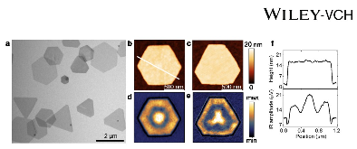
Topological insulators (TIs) are quantum materials with topologically protected surface states surrounding an insulating bulk. However, defect-induced bulk conduction often dominates transport properties in most TI materials, obscuring the Dirac surface states. In order to realize intrinsic topological insulating properties, it is thus of great significance to identify the spatial distribution of defects, understand their formation mechanism, and finally control or eliminate their influence. For this study, the electronic heterogeneity in polyol-synthesized Bi2Se3 and chemical vapor deposition-grown Sb2 Te3 nanocrystals is systematically investigated by multimodal atomic-to-mesoscale resolution imaging. In particular, by combining the Drude response sensitivity of infrared scattering-type scanning near-field optical microscopy with the work-function specificity of mirror electron microscopy, characteristic mesoscopic patterns are identified, which are related to carrier concentration modulation originating from the formation of defects during the crystal growth process. This correlative imaging and modeling approach thus provides the desired guidance for optimization of growth parameters, crucial for preparing TI nanomaterials to display their intrinsic exotic Dirac properties.
- Research Organization:
- Lawrence Berkeley National Laboratory (LBNL), Berkeley, CA (United States)
- Sponsoring Organization:
- USDOE Office of Science (SC), Basic Energy Sciences (BES) (SC-22). Materials Sciences & Engineering Division; National Key Research and Development Program of China; National Natural Science Foundation of China (NSFC); National Science Foundation (NSF)
- Grant/Contract Number:
- AC02-05CH11231; 2016YFA0203500; 51290272; 11474350; SC0008807; DMR‐1548924
- OSTI ID:
- 1432242
- Alternate ID(s):
- OSTI ID: 1412594
- Journal Information:
- Advanced Electronic Materials, Vol. 4, Issue 1; Related Information: © 2017 WILEY-VCH Verlag GmbH & Co. KGaA, Weinheim; ISSN 2199-160X
- Publisher:
- WileyCopyright Statement
- Country of Publication:
- United States
- Language:
- English
Web of Science


Similar Records
Real-space nanoimaging of THz polaritons in the topological insulator Bi2Se3
Absence of a Dirac gap in ferromagnetic Crx(Bi0.1Sb0.9)2-xTe3