Microchannel contacting of crystalline silicon solar cells
Journal Article
·
· Scientific Reports
- Univ. of California, Berkeley, CA (United States); Lawrence Berkeley National Lab. (LBNL), Berkeley, CA (United States)
- The Australian National Univ., Canberra, ACT (Australia)
- Ecole Polytechnique Federale de Lausanne (EPFL), Neuchatel (Switzerland)
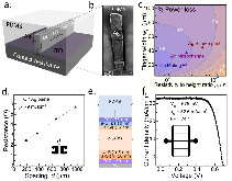
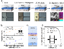
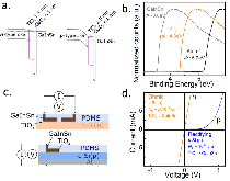
There is tremendous interest in reducing losses caused by the metal contacts in silicon photovoltaics, particularly the optical and resistive losses of the front metal grid. One commonly sought-after goal is the creation of high aspect-ratio metal fingers which provide an optically narrow and low resistance pathway to the external circuit. Currently, the most widely used metal contact deposition techniques are limited to widths and aspect-ratios of ~40 μm and ~0.5, respectively. In this study, we introduce the use of a micropatterned polydimethylsiloxane encapsulation layer to form narrow (~20 μm) microchannels, with aspect-ratios up to 8, on the surface of solar cells. We demonstrate that low temperature metal pastes, electroless plating and atomic layer deposition can all be used within the microchannels. Further, we fabricate proof-of-concept structures including simple planar silicon heterojunction and homojunction solar cells. While preliminary in both design and efficiency, these results demonstrate the potential of this approach and its compatibility with current solar cell architectures.
- Research Organization:
- Lawrence Berkeley National Laboratory (LBNL), Berkeley, CA (United States)
- Sponsoring Organization:
- USDOE Office of Science (SC), Basic Energy Sciences (BES) (SC-22)
- Grant/Contract Number:
- AC02-05CH11231
- OSTI ID:
- 1417622
- Journal Information:
- Scientific Reports, Journal Name: Scientific Reports Journal Issue: 1 Vol. 7; ISSN 2045-2322
- Publisher:
- Nature Publishing GroupCopyright Statement
- Country of Publication:
- United States
- Language:
- English
Assessment of the energy recovery potential of waste Photovoltaic (PV) modules
|
journal | March 2019 |

Similar Records
Novel buried contact technology for advanced silicon solar cells
In situ recombination junction between p-Si and TiO2 enables high-efficiency monolithic perovskite/Si tandem cells
Book
·
Fri Dec 30 23:00:00 EST 1994
·
OSTI ID:191058
In situ recombination junction between p-Si and TiO2 enables high-efficiency monolithic perovskite/Si tandem cells
Journal Article
·
Thu Dec 13 19:00:00 EST 2018
· Science Advances
·
OSTI ID:1610792