Massachusetts Inst. of Technology (MIT), Cambridge, MA (United States). Research Lab. of Electronics; Trinity College, Dublin (Ireland). Centre for Research on Adapative Nanostructures and Nanodevices (CRANN), Advanced Materials Bio-Engineering Resarch Center (AMBER); Massachusetts Institute of Technology
Massachusetts Inst. of Technology (MIT), Cambridge, MA (United States). Research Lab. of Electronics; Univ. of Hamburg (Germany). Dept. of Physics, Center for Ultrafast Imaging; Northrop Grumman, Redondo Beach, CA (United States)
Deutsches Elektronen-Synchrotron (DESY), Hamburg (Germany). Center for Free-Electron Laser Science
Massachusetts Inst. of Technology (MIT), Cambridge, MA (United States). Research Lab. of Electronics
Massachusetts Inst. of Technology (MIT), Cambridge, MA (United States). Research Lab. of Electronics; Univ. of Hamburg (Germany). Dept. of Physics, Center for Ultrafast Imaging; Deutsches Elektronen-Synchrotron (DESY), Hamburg (Germany). Center for Free-Electron Laser Science
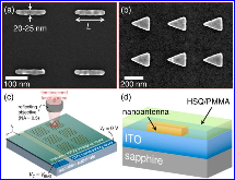
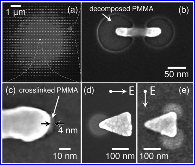
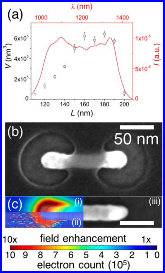
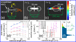
Understanding plasmon-mediated electron emission and energy transfer on the nanometer length scale is critical to controlling light–matter interactions at nanoscale dimensions. In a high-resolution lithographic material, electron emission and energy transfer lead to chemical transformations. Here, we employ such chemical transformations in two different high-resolution electron-beam lithography resists, poly(methyl methacrylate) (PMMA) and hydrogen silsesquioxane (HSQ), to map local electron emission and energy transfer with nanometer resolution from plasmonic nanoantennas excited by femtosecond laser pulses. We observe exposure of the electron-beam resists (both PMMA and HSQ) in regions on the surface of nanoantennas where the local field is significantly enhanced. Exposure in these regions is consistent with previously reported optical-field-controlled electron emission from plasmonic hotspots as well as earlier work on low-electron-energy scanning probe lithography. For HSQ, in addition to exposure in hotspots, we observe resist exposure at the centers of rod-shaped nanoantennas in addition to exposure in plasmonic hotspots. Optical field enhancement is minimized at the center of nanorods suggesting that exposure in these regions involves a different mechanism to that in plasmonic hotspots. Our simulations suggest that exposure at the center of nanorods results from the emission of hot electrons produced via plasmon decay in the nanorods. Our results provide a means to map both optical-field-controlled electron emission and hot-electron transfer from nanoparticles via chemical transformations produced locally in lithographic materials.
Hobbs, Richard G., et al. "Mapping Photoemission and Hot-Electron Emission from Plasmonic Nanoantennas." Nano Letters, vol. 17, Sep. 2017. https://doi.org/10.1021/acs.nanolett.7b02495
Hobbs, Richard G., Putnam, William P., Fallahi, Arya, Yang, Yujia, Kärtner, Franz X., & Berggren, Karl K. (2017). Mapping Photoemission and Hot-Electron Emission from Plasmonic Nanoantennas. Nano Letters, 17. https://doi.org/10.1021/acs.nanolett.7b02495
Hobbs, Richard G., Putnam, William P., Fallahi, Arya, et al., "Mapping Photoemission and Hot-Electron Emission from Plasmonic Nanoantennas," Nano Letters 17 (2017), https://doi.org/10.1021/acs.nanolett.7b02495
@article{osti_1395006,
  author       = {Hobbs, Richard G. and Putnam, William P. and Fallahi, Arya and Yang, Yujia and Kärtner, Franz X. and Berggren, Karl K.},
  title        = {Mapping Photoemission and Hot-Electron Emission from Plasmonic Nanoantennas},
  annote       = {Understanding plasmon-mediated electron emission and energy transfer on the nanometer length scale is critical to controlling light–matter interactions at nanoscale dimensions. In a high-resolution lithographic material, electron emission and energy transfer lead to chemical transformations. Here, we employ such chemical transformations in two different high-resolution electron-beam lithography resists, poly(methyl methacrylate) (PMMA) and hydrogen silsesquioxane (HSQ), to map local electron emission and energy transfer with nanometer resolution from plasmonic nanoantennas excited by femtosecond laser pulses. We observe exposure of the electron-beam resists (both PMMA and HSQ) in regions on the surface of nanoantennas where the local field is significantly enhanced. Exposure in these regions is consistent with previously reported optical-field-controlled electron emission from plasmonic hotspots as well as earlier work on low-electron-energy scanning probe lithography. For HSQ, in addition to exposure in hotspots, we observe resist exposure at the centers of rod-shaped nanoantennas in addition to exposure in plasmonic hotspots. Optical field enhancement is minimized at the center of nanorods suggesting that exposure in these regions involves a different mechanism to that in plasmonic hotspots. Our simulations suggest that exposure at the center of nanorods results from the emission of hot electrons produced via plasmon decay in the nanorods. Our results provide a means to map both optical-field-controlled electron emission and hot-electron transfer from nanoparticles via chemical transformations produced locally in lithographic materials.},
  doi          = {10.1021/acs.nanolett.7b02495},
  url          = {https://www.osti.gov/biblio/1395006},
  journal      = {Nano Letters},
  issn         = {ISSN 1530-6984},
  volume       = {17},
  place        = {United States},
  publisher    = {American Chemical Society},
  year         = {2017},
  month        = {09}}