
Observation and mitigation of RF-plasma-induced damage to III-nitrides grown by molecular beam epitaxy
Abstract
In this work, radio-frequency (RF) plasma-induced damage to III-nitride surfaces and bulk defects is observed and mitigated. It is shown that for InN films, the surface is more sensitive to plasma-induced damage than GaN films, as observed via atomic force microscopy and reflection high energy electron diffraction. In order to isolate any possible plasma-induced damage, a growth window for InN is established, and temperature ranges are determined for other damaging effects which include roughening due to low adatom mobility, InN decomposition, and indium desorption. In situ plasma monitoring and optimization are accomplished with a combination of optical emission spectroscopy as well as a remote Langmuir probe. It is shown that by increasing the plasma nitrogen flow, the positive ion content increases; however, the ion acceleration potential reduces. Additionally, a reduced RF plasma power results in a reduction of atomic nitrogen species. These plasma species and energetic variations result in variations in the bulk unintentional background electron concentrations observed by room temperature Hall effect measurements of ~1 um thick InN films. By increasing the nitrogen flow from 2.5 to 7.5 sccm for a constant RF power of 350 W, the background electron concentration decreases by 74% from 1.36 x 1019 cm-3more »
- Authors:
-
 [1];
[1];
[2];
[1];
[1];
[2];
- Georgia Inst. of Technology, Atlanta, GA (United States)
- National Renewable Energy Lab. (NREL), Golden, CO (United States)
- Publication Date:
- Research Org.:
- National Renewable Energy Lab. (NREL), Golden, CO (United States)
- Sponsoring Org.:
- USDOE Advanced Research Projects Agency - Energy (ARPA-E)
- OSTI Identifier:
- 1545263
- Alternate Identifier(s):
- OSTI ID: 1530634
- Report Number(s):
- NREL/JA-5K00-74387
Journal ID: ISSN 0021-8979
- Grant/Contract Number:
- AC36-08GO28308; DEAR0000470
- Resource Type:
- Accepted Manuscript
- Journal Name:
- Journal of Applied Physics
- Additional Journal Information:
- Journal Volume: 126; Journal Issue: 1; Journal ID: ISSN 0021-8979
- Publisher:
- American Institute of Physics (AIP)
- Country of Publication:
- United States
- Language:
- English
- Subject:
- 36 MATERIALS SCIENCE; 71 CLASSICAL AND QUANTUM MECHANICS, GENERAL PHYSICS; epitaxy; nitrides; optical emission spectroscopy; surface and interface chemistry; plasma diagnostics; photoluminescence spectroscopy
Citation Formats
                    Clinton, Evan A., Vadiee, Ehsan, Tellekamp, M. Brooks, and Doolittle, W. Alan. Observation and mitigation of RF-plasma-induced damage to III-nitrides grown by molecular beam epitaxy.  United States: N. p., 2019.
Web.  doi:10.1063/1.5097557.
Clinton, Evan A., Vadiee, Ehsan, Tellekamp, M. Brooks, & Doolittle, W. Alan. Observation and mitigation of RF-plasma-induced damage to III-nitrides grown by molecular beam epitaxy. United States. https://doi.org/10.1063/1.5097557
                    Clinton, Evan A., Vadiee, Ehsan, Tellekamp, M. Brooks, and Doolittle, W. Alan. Tue .
"Observation and mitigation of RF-plasma-induced damage to III-nitrides grown by molecular beam epitaxy".  United States.  https://doi.org/10.1063/1.5097557.  https://www.osti.gov/servlets/purl/1545263.
@article{osti_1545263,

  title        = {Observation and mitigation of RF-plasma-induced damage to III-nitrides grown by molecular beam epitaxy},

  author       = {Clinton, Evan A. and Vadiee, Ehsan and Tellekamp, M. Brooks and Doolittle, W. Alan},

  abstractNote = {In this work, radio-frequency (RF) plasma-induced damage to III-nitride surfaces and bulk defects is observed and mitigated. It is shown that for InN films, the surface is more sensitive to plasma-induced damage than GaN films, as observed via atomic force microscopy and reflection high energy electron diffraction. In order to isolate any possible plasma-induced damage, a growth window for InN is established, and temperature ranges are determined for other damaging effects which include roughening due to low adatom mobility, InN decomposition, and indium desorption. In situ plasma monitoring and optimization are accomplished with a combination of optical emission spectroscopy as well as a remote Langmuir probe. It is shown that by increasing the plasma nitrogen flow, the positive ion content increases; however, the ion acceleration potential reduces. Additionally, a reduced RF plasma power results in a reduction of atomic nitrogen species. These plasma species and energetic variations result in variations in the bulk unintentional background electron concentrations observed by room temperature Hall effect measurements of ~1 um thick InN films. By increasing the nitrogen flow from 2.5 to 7.5 sccm for a constant RF power of 350 W, the background electron concentration decreases by 74% from 1.36 x 1019 cm-3 to 3.54 x 1018 cm-3, while maintaining a smooth surface morphology. Additionally, photoluminescence spectra indicate optical emission energies shift from ~0.81 to 0.71 eV (closer to the fundamental bandgap of InN) by limiting the damaging plasma species. Finally, conditions are presented to further minimize plasma-induced damage in III-nitride devices.},

  doi          = {10.1063/1.5097557},

  journal      = {Journal of Applied Physics},

  number       = 1,

  volume       = 126,

  place        = {United States},

  year         = {Tue Jul 02 00:00:00 EDT 2019},

  month        = {Tue Jul 02 00:00:00 EDT 2019}

}
 Search WorldCat to find libraries that may hold this journal
Web of Science
Figures / Tables:
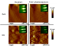 Figure 1: AFM images of as-grown and post-growth plasma exposed GaN and InN films. The InN surface is degraded by plasma exposure (inset: associated RHEED images.)
Works referenced in this record:
The Interpretation of the Properties of Indium Antimonide
journal, October 1954
- Moss, T. S.
- Proceedings of the Physical Society. Section B, Vol. 67, Issue 10
Guidelines and limitations for the design of high-efficiency InGaN single-junction solar cells
journal, November 2014
- Fabien, Chloe A. M.; Doolittle, W. Alan
- Solar Energy Materials and Solar Cells, Vol. 130
Thermodynamical properties of III–V nitrides and crystal growth of GaN at high N2 pressure
journal, June 1997
- Porowski, S.; Grzegory, I.
- Journal of Crystal Growth, Vol. 178, Issue 1-2
Langmuir probe technique for plasma parameter measurement in a medium density discharge
journal, September 1986
- Hopkins, M. B.; Graham, W. G.
- Review of Scientific Instruments, Vol. 57, Issue 9
Structural and electrical characterization of InN, InGaN, and p-InGaN grown by metal-modulated epitaxy
journal, May 2013
- Moseley, Michael; Gunning, Brendan; Lowder, Jonathan
- Journal of Vacuum Science & Technology B, Nanotechnology and Microelectronics: Materials, Processing, Measurement, and Phenomena, Vol. 31, Issue 3
Nitrogen species from radio frequency plasma sources used for molecular beam epitaxy growth of GaN
journal, January 2000
- Blant, A. V.; Hughes, O. H.; Cheng, T. S.
- Plasma Sources Science and Technology, Vol. 9, Issue 1
Acceptor states in the photoluminescence spectra of
journal, May 2005
- Klochikhin, A. A.; Davydov, V. Yu.; Emtsev, V. V.
- Physical Review B, Vol. 71, Issue 19
Control of ion content and nitrogen species using a mixed chemistry plasma for GaN grown at extremely high growth rates >9 μ m/h by plasma-assisted molecular beam epitaxy
journal, October 2015
- Gunning, Brendan P.; Clinton, Evan A.; Merola, Joseph J.
- Journal of Applied Physics, Vol. 118, Issue 15
Optical bandgap energy of wurtzite InN
journal, August 2002
- Matsuoka, Takashi; Okamoto, Hiroshi; Nakao, Masashi
- Applied Physics Letters, Vol. 81, Issue 7
A growth diagram for plasma-assisted molecular beam epitaxy of In-face InN
journal, September 2007
- Gallinat, C. S.; Koblmüller, G.; Brown, J. S.
- Journal of Applied Physics, Vol. 102, Issue 6
Simulations, Practical Limitations, and Novel Growth Technology for InGaN-Based Solar Cells
journal, March 2014
- Fabien, Chloe A. M.; Moseley, Michael; Gunning, Brendan
- IEEE Journal of Photovoltaics, Vol. 4, Issue 2
Superior radiation resistance of In1−xGaxN alloys: Full-solar-spectrum photovoltaic material system
journal, November 2003
- Wu, J.; Walukiewicz, W.; Yu, K. M.
- Journal of Applied Physics, Vol. 94, Issue 10
Energy position of near-band-edge emission spectra of InN epitaxial layers with different doping levels
journal, March 2004
- Arnaudov, B.; Paskova, T.; Paskov, P. P.
- Physical Review B, Vol. 69, Issue 11
InGaN solar cells with regrown GaN homojunction tunnel contacts
journal, July 2018
- Vadiee, Ehsan; Clinton, Evan A.; McFavilen, Heather
- Applied Physics Express, Vol. 11, Issue 8
Band Gap of Hexagonal InN and InGaN Alloys
journal, December 2002
- Davydov, V. Yu.; Klochikhin, A. A.; Emtsev, V. V.
- physica status solidi (b), Vol. 234, Issue 3
Development of a high-band gap high temperature III-nitride solar cell for integration with concentrated solar power technology
conference, June 2016
- Williams, Joshua J.; McFavilen, Heather; Fischer, Alec M.
- 2016 IEEE 43rd Photovoltaic Specialists Conference (PVSC)
Understanding Langmuir probe current-voltage characteristics
journal, December 2007
- Merlino, Robert L.
- American Journal of Physics, Vol. 75, Issue 12
Four free parameter empirical parametrization of glow discharge Langmuir probe data
journal, October 2008
- Azooz, A. A.
- Review of Scientific Instruments, Vol. 79, Issue 10
Refractory In$_{x}$ Ga1−$_{x}$ N Solar Cells for High-Temperature Applications
journal, November 2017
- Williams, Joshua J.; Goodnick, Stephen M.; McFavilen, Heather
- IEEE Journal of Photovoltaics, Vol. 7, Issue 6
Intrinsic Electron Accumulation at Clean InN Surfaces
journal, January 2004
- Mahboob, I.; Veal, T. D.; McConville, C. F.
- Physical Review Letters, Vol. 92, Issue 3
The relation of active nitrogen species to high-temperature limitations for (0001̄) GaN growth by radio-frequency-plasma-assisted molecular beam epitaxy
journal, June 1999
- Ptak, A. J.; Millecchia, M. R.; Myers, T. H.
- Applied Physics Letters, Vol. 74, Issue 25
Absorption coefficient, energy gap, exciton binding energy, and recombination lifetime of GaN obtained from transmission measurements
journal, November 1997
- Muth, J. F.; Lee, J. H.; Shmagin, I. K.
- Applied Physics Letters, Vol. 71, Issue 18
Control of surface adatom kinetics for the growth of high-indium content InGaN throughout the miscibility gap
journal, November 2010
- Moseley, Michael; Lowder, Jonathan; Billingsley, Daniel
- Applied Physics Letters, Vol. 97, Issue 19
Active nitrogen species dependence on radiofrequency plasma source operating parameters and their role in GaN growth
journal, May 2005
- Iliopoulos, E.; Adikimenakis, A.; Dimakis, E.
- Journal of Crystal Growth, Vol. 278, Issue 1-4
Unusual properties of the fundamental band gap of InN
journal, May 2002
- Wu, J.; Walukiewicz, W.; Yu, K. M.
- Applied Physics Letters, Vol. 80, Issue 21
III-Nitride Double-Heterojunction Solar Cells With High In-Content InGaN Absorbing Layers: Comparison of Large-Area and Small-Area Devices
journal, March 2016
- Fabien, Chloe A. M.; Maros, Aymeric; Honsberg, Christiana B.
- IEEE Journal of Photovoltaics, Vol. 6, Issue 2
Fundamentals, Material Properties and Device Performances in GaN MBE using On-Surface Cracking of Ammonia
journal, January 1997
- Kamp, Markus; Mayer, M.; Pelzmann, A.
- MRS Internet Journal of Nitride Semiconductor Research, Vol. 2
Low-temperature growth of InGaN films over the entire composition range by MBE
journal, September 2015
- Fabien, Chloe A. M.; Gunning, Brendan P.; Alan Doolittle, W.
- Journal of Crystal Growth, Vol. 425
Transient atomic behavior and surface kinetics of GaN
journal, July 2009
- Moseley, Michael; Billingsley, Daniel; Henderson, Walter
- Journal of Applied Physics, Vol. 106, Issue 1
Mahan excitons in degenerate wurtzite InN: Photoluminescence spectroscopy and reflectivity measurements
journal, June 2008
- Feneberg, Martin; Däubler, Jürgen; Thonke, Klaus
- Physical Review B, Vol. 77, Issue 24
High-performance broadband optical coatings on InGaN/GaN solar cells for multijunction device integration
journal, April 2014
- Young, N. G.; Perl, E. E.; Farrell, R. M.
- Applied Physics Letters, Vol. 104, Issue 16
A review of the synthesis of reduced defect density InxGa1−xN for all indium compositions
journal, October 2017
- Clinton, Evan A.; Vadiee, Ehsan; Fabien, Chloe A. M.
- Solid-State Electronics, Vol. 136
Figures / Tables found in this record: