
Persistent Charge-Density-Wave Order in Single-Layer TaSe 2
Abstract
We present the electronic characterization of single-layer 1H-TaSe2 grown by molecular beam epitaxy using a combined angle-resolved photoemission spectroscopy, scanning tunneling microscopy/spectroscopy, and density functional theory calculations. We demonstrate that 3 × 3 charge-density-wave (CDW) order persists despite distinct changes in the low energy electronic structure highlighted by the reduction in the number of bands crossing the Fermi energy and the corresponding modification of Fermi surface topology. Enhanced spin-orbit coupling and lattice distortion in the single-layer play a crucial role in the formation of CDW order. Our findings provide a deeper understanding of the nature of CDW order in the two-dimensional limit.
- Authors:
-
 [1];
[5];
[9];
[5]
[1];
[5];
[9];
[5]
- Lawrence Berkeley National Lab. (LBNL), Berkeley, CA (United States); Pohang Univ. of Science and Technology, Pohang (Korea)
- Univ. of California, Berkeley, CA (United States)
- Pohang Univ. of Science and Technology, Pohang (Korea)
- Lawrence Berkeley National Lab. (LBNL), Berkeley, CA (United States); SLAC National Accelerator Lab., Menlo Park, CA (United States)
- Lawrence Berkeley National Lab. (LBNL), Berkeley, CA (United States)
- Univ. of California, Berkeley, CA (United States); Henan Univ., Keifeng (People's Republic of China)
- Lawrence Berkeley National Lab. (LBNL), Berkeley, CA (United States); Stanford Univ., Stanford, CA (United States)
- Pusan National Univ., Busan (Korea)
- Univ. of California, Berkeley, CA (United States); Lawrence Berkeley National Lab. (LBNL), Berkeley, CA (United States)
- Publication Date:
- Research Org.:
- SLAC National Accelerator Lab., Menlo Park, CA (United States); Lawrence Berkeley National Lab. (LBNL), Berkeley, CA (United States). Advanced Light Source; Lawrence Berkeley National Lab. (LBNL), Berkeley, CA (United States)
- Sponsoring Org.:
- USDOE Office of Science (SC), Basic Energy Sciences (BES)
- OSTI Identifier:
- 1471522
- Alternate Identifier(s):
- OSTI ID: 1471447; OSTI ID: 1530339
- Grant/Contract Number:
- AC02-76SF00515; 2015R1A2A1A15053564; 2016K1A4A4A01922028; AC02-05CH11231
- Resource Type:
- Accepted Manuscript
- Journal Name:
- Nano Letters
- Additional Journal Information:
- Journal Volume: 18; Journal Issue: 2; Journal ID: ISSN 1530-6984
- Publisher:
- American Chemical Society
- Country of Publication:
- United States
- Language:
- English
- Subject:
- 74 ATOMIC AND MOLECULAR PHYSICS; 2D materials; ARPES; CDW; charge density wave; MBE; STM; TaSe2; Transition metal dichalcogenides; 36 MATERIALS SCIENCE
Citation Formats
                    Ryu, Hyejin, Chen, Yi, Kim, Heejung, Tsai, Hsin -Zon, Tang, Shujie, Jiang, Juan, Liou, Franklin, Kahn, Salman, Jia, Caihong, Omrani, Arash A., Shim, Ji Hoon, Hussain, Zahid, Shen, Zhi -Xun, Kim, Kyoo, Min, Byung Il, Hwang, Choongyu, Crommie, Michael F., and Mo, Sung -Kwan. Persistent Charge-Density-Wave Order in Single-Layer TaSe 2.  United States: N. p., 2018.
Web.  doi:10.1021/acs.nanolett.7b03264.
Ryu, Hyejin, Chen, Yi, Kim, Heejung, Tsai, Hsin -Zon, Tang, Shujie, Jiang, Juan, Liou, Franklin, Kahn, Salman, Jia, Caihong, Omrani, Arash A., Shim, Ji Hoon, Hussain, Zahid, Shen, Zhi -Xun, Kim, Kyoo, Min, Byung Il, Hwang, Choongyu, Crommie, Michael F., & Mo, Sung -Kwan. Persistent Charge-Density-Wave Order in Single-Layer TaSe 2. United States. https://doi.org/10.1021/acs.nanolett.7b03264
                    Ryu, Hyejin, Chen, Yi, Kim, Heejung, Tsai, Hsin -Zon, Tang, Shujie, Jiang, Juan, Liou, Franklin, Kahn, Salman, Jia, Caihong, Omrani, Arash A., Shim, Ji Hoon, Hussain, Zahid, Shen, Zhi -Xun, Kim, Kyoo, Min, Byung Il, Hwang, Choongyu, Crommie, Michael F., and Mo, Sung -Kwan. Thu .
"Persistent Charge-Density-Wave Order in Single-Layer TaSe 2".  United States.  https://doi.org/10.1021/acs.nanolett.7b03264.  https://www.osti.gov/servlets/purl/1471522.
@article{osti_1471522,

  title        = {Persistent Charge-Density-Wave Order in Single-Layer TaSe 2},

  author       = {Ryu, Hyejin and Chen, Yi and Kim, Heejung and Tsai, Hsin -Zon and Tang, Shujie and Jiang, Juan and Liou, Franklin and Kahn, Salman and Jia, Caihong and Omrani, Arash A. and Shim, Ji Hoon and Hussain, Zahid and Shen, Zhi -Xun and Kim, Kyoo and Min, Byung Il and Hwang, Choongyu and Crommie, Michael F. and Mo, Sung -Kwan},

  abstractNote = {We present the electronic characterization of single-layer 1H-TaSe2 grown by molecular beam epitaxy using a combined angle-resolved photoemission spectroscopy, scanning tunneling microscopy/spectroscopy, and density functional theory calculations. We demonstrate that 3 × 3 charge-density-wave (CDW) order persists despite distinct changes in the low energy electronic structure highlighted by the reduction in the number of bands crossing the Fermi energy and the corresponding modification of Fermi surface topology. Enhanced spin-orbit coupling and lattice distortion in the single-layer play a crucial role in the formation of CDW order. Our findings provide a deeper understanding of the nature of CDW order in the two-dimensional limit.},

  doi          = {10.1021/acs.nanolett.7b03264},

  journal      = {Nano Letters},

  number       = 2,

  volume       = 18,

  place        = {United States},

  year         = {Thu Jan 04 00:00:00 EST 2018},

  month        = {Thu Jan 04 00:00:00 EST 2018}

}
 Search WorldCat to find libraries that may hold this journal
Web of Science
Figures / Tables:
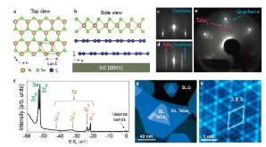 Figure 1.: Growth of epitaxial single-layer 1H-TaSe2 film. (a) Crystal structure 1H-TaSe2 single-layer film on bilayer graphene 6H-SiC(0001) from top view and (b) side view. (c) RHEED pattern of epitaxial bilayer graphene on 6H-SiC(0001) substrate and (d) 0.9 monolayer (ML, 0.9 ML means that 90% area of the substrate surfacemore »
Works referenced in this record:
Synthesis and chemistry of elemental 2D materials
journal, January 2017
- Mannix, Andrew J.; Kiraly, Brian; Hersam, Mark C.
- Nature Reviews Chemistry, Vol. 1, Issue 2
Two-dimensional semiconductors for transistors
journal, August 2016
- Chhowalla, Manish; Jena, Debdeep; Zhang, Hua
- Nature Reviews Materials, Vol. 1, Issue 11
2D materials and van der Waals heterostructures
journal, July 2016
- Novoselov, K. S.; Mishchenko, A.; Carvalho, A.
- Science, Vol. 353, Issue 6298
On the origin of charge-density waves in select layered transition-metal dichalcogenides
journal, May 2011
- Rossnagel, K.
- Journal of Physics: Condensed Matter, Vol. 23, Issue 21
Charge Density Wave, Superconductivity, and Anomalous Metallic Behavior in 2D Transition Metal Dichalcogenides
journal, May 2001
- Castro Neto, A. H.
- Physical Review Letters, Vol. 86, Issue 19
The dynamics of charge-density waves
journal, October 1988
- Grüner, G.
- Reviews of Modern Physics, Vol. 60, Issue 4
Quasiparticle Interference, Quasiparticle Interactions, and the Origin of the Charge Density Wave in
journal, January 2015
- Arguello, C. J.; Rosenthal, E. P.; Andrade, E. F.
- Physical Review Letters, Vol. 114, Issue 3
-resolved susceptibility function of 2 -TaSe from angle-resolved photoemission
journal, July 2013
- Laverock, J.; Newby, D.; Abreu, E.
- Physical Review B, Vol. 88, Issue 3
Fermi-surface nesting and the origin of the charge-density wave in
journal, May 2006
- Johannes, M.; Mazin, I.; Howells, C.
- Physical Review B, Vol. 73, Issue 20
Characterization of collective ground states in single-layer NbSe2
journal, November 2015
- Ugeda, Miguel M.; Bradley, Aaron J.; Zhang, Yi
- Nature Physics, Vol. 12, Issue 1
Spin–valley locking in the normal state of a transition-metal dichalcogenide superconductor
journal, May 2016
- Bawden, L.; Cooil, S. P.; Mazzola, F.
- Nature Communications, Vol. 7, Issue 1
Strongly enhanced charge-density-wave order in monolayer NbSe2
journal, July 2015
- Xi, Xiaoxiang; Zhao, Liang; Wang, Zefang
- Nature Nanotechnology, Vol. 10, Issue 9, p. 765-769
Ising pairing in superconducting NbSe2 atomic layers
journal, November 2015
- Xi, Xiaoxiang; Wang, Zefang; Zhao, Weiwei
- Nature Physics, Vol. 12, Issue 2
Charge density waves and superconductivity in 2H-TaSe2
journal, May 1996
- Kumakura, Tomohisa; Tan, Hiroki; Handa, Tetsuya
- Czechoslovak Journal of Physics, Vol. 46, Issue S5
Na and Cs intercalation of 2H-TaSe 2 studied by photoemission
journal, October 2001
- Brauer, H. E.; Starnberg, H. I.; Holleboom, L. J.
- Journal of Physics: Condensed Matter, Vol. 13, Issue 44
Pseudogap and Charge Density Waves in Two Dimensions
journal, May 2008
- Borisenko, S. V.; Kordyuk, A. A.; Yaresko, A. N.
- Physical Review Letters, Vol. 100, Issue 19
Effect of dimensionality and spin-orbit coupling on charge-density-wave transition in 2H-TaSe
journal, September 2012
- Ge, Yizhi; Liu, Amy Y.
- Physical Review B, Vol. 86, Issue 10
Fermi surface, charge-density-wave gap, and kinks in
journal, September 2005
- Rossnagel, K.; Rotenberg, Eli; Koh, H.
- Physical Review B, Vol. 72, Issue 12
Accurate Band Gaps of Semiconductors and Insulators with a Semilocal Exchange-Correlation Potential
journal, June 2009
- Tran, Fabien; Blaha, Peter
- Physical Review Letters, Vol. 102, Issue 22
A simple effective potential for exchange
journal, June 2006
- Becke, Axel D.; Johnson, Erin R.
- The Journal of Chemical Physics, Vol. 124, Issue 22
Charge density wave transition in single-layer titanium diselenide
journal, November 2015
- Chen, P.; Chan, Y. -H.; Fang, X. -Y.
- Nature Communications, Vol. 6, Issue 1
Study of Superlattice Formation in -Nb and -Ta by Neutron Scattering
journal, March 1975
- Moncton, D. E.; Axe, J. D.; DiSalvo, F. J.
- Physical Review Letters, Vol. 34, Issue 12
Quantum phase transition from triangular to stripe charge order in NbSe2
journal, January 2013
- Soumyanarayanan, A.; Yee, M. M.; He, Y.
- Proceedings of the National Academy of Sciences, Vol. 110, Issue 5
Scanning tunnelling microscopy of charge-density waves in transition metal chalcogenides
journal, December 1988
- Coleman, R. V.; Giambattista, B.; Hansma, P. K.
- Advances in Physics, Vol. 37, Issue 6
Superconductivity at the Two-Dimensional Limit
journal, April 2009
- Qin, S.; Kim, J.; Niu, Q.
- Science, Vol. 324, Issue 5932
Giant phonon-induced conductance in scanning tunnelling spectroscopy of gate-tunable graphene
journal, July 2008
- Zhang, Yuanbo; Brar, Victor W.; Wang, Feng
- Nature Physics, Vol. 4, Issue 8
Theory and Application for the Scanning Tunneling Microscope
journal, June 1983
- Tersoff, J.; Hamann, D. R.
- Physical Review Letters, Vol. 50, Issue 25
Large-scale uniform bilayer graphene prepared by vacuum graphitization of 6H-SiC(0001) substrates
journal, January 2013
- Wang, Qingyan; Zhang, Wenhao; Wang, Lili
- Journal of Physics: Condensed Matter, Vol. 25, Issue 9
Unfolding First-Principles Band Structures
journal, May 2010
- Ku, Wei; Berlijn, Tom; Lee, Chi-Cheng
- Physical Review Letters, Vol. 104, Issue 21
Works referencing / citing this record:
Single anisotropic gap superconductivity and proximity effect in
journal, December 2019
- Lian, Chao-Sheng; Si, Chen; Duan, Wenhui
- Physical Review B, Vol. 100, Issue 23
Distinctive Performance of Terahertz Photodetection Driven by Charge‐Density‐Wave Order in CVD‐Grown Tantalum Diselenide
journal, September 2019
- Wang, Lin; Wang, Jin; Liu, Changlong
- Advanced Functional Materials, Vol. 29, Issue 45
The Computational 2D Materials Database: high-throughput modeling and discovery of atomically thin crystals
journal, September 2018
- Haastrup, Sten; Strange, Mikkel; Pandey, Mohnish
- 2D Materials, Vol. 5, Issue 4
Morphology‐controlled Tantalum Diselenide Structures as Self‐optimizing Hydrogen Evolution Catalysts
journal, March 2020
- Wang, Min; Zhang, Li; Huang, Meirong
- ENERGY & ENVIRONMENTAL MATERIALS, Vol. 3, Issue 1
Strong correlations and orbital texture in single-layer 1T-TaSe2
journal, January 2020
- Chen, Yi; Ruan, Wei; Wu, Meng
- Nature Physics, Vol. 16, Issue 2
Charge Order of Strongly Bounded Electron Pairs on the Triangular Lattice: the Zero-Bandwidth Limit of the Extended Hubbard Model with Strong Onsite Attraction
journal, March 2019
- Kapcia, Konrad Jerzy
- Journal of Superconductivity and Novel Magnetism, Vol. 32, Issue 9
2DMatPedia, an open computational database of two-dimensional materials from top-down and bottom-up approaches
journal, June 2019
- Zhou, Jun; Shen, Lei; Costa, Miguel Dias
- Scientific Data, Vol. 6, Issue 1
Role of Charge Density Wave in Monatomic Assembly in Transition Metal Dichalcogenides
journal, February 2019
- Feng, Haifeng; Xu, Zhongfei; Zhuang, Jincheng
- Advanced Functional Materials, Vol. 29, Issue 15
Chemical Vapor Deposition Grown Wafer-Scale 2D Tantalum Diselenide with Robust Charge-Density-Wave Order
journal, September 2018
- Shi, Jianping; Chen, Xuexian; Zhao, Liyun
- Advanced Materials, Vol. 30, Issue 44
Strain-controlled magnetic and optical properties of monolayer
journal, August 2019
- Chowdhury, Sugata; Simpson, Jeffrey R.; Einstein, T. L.
- Physical Review Materials, Vol. 3, Issue 8
Multivalley Free Energy Landscape and the Origin of Stripe and Quasi-Stripe CDW Structures in Monolayer MX2 Compounds
journal, January 2020
- Nakatsugawa, Keiji; Tanda, Satoshi; Ikeda, Tatsuhiko N.
- Scientific Reports, Vol. 10, Issue 1
In situ electrodeposition of polypyrrole onto TaSe 2 nanobelts quasi-arrays for high-capacitance supercapacitor
journal, January 2018
- Wang, Min; Zhang, Li; Zhong, Yujia
- Nanoscale, Vol. 10, Issue 36
Dimensional reduction and ionic gating induced enhancement of superconductivity in atomically thin crystals of 2H-TaSe 2
journal, November 2018
- Wu, Yueshen; He, Jiaming; Liu, Jinyu
- Nanotechnology, Vol. 30, Issue 3
Real-space investigation of the charge density wave in monolayer with broken rotational and mirror symmetries
journal, January 2020
- Miao, Guangyao; Xue, Siwei; Li, Bo
- Physical Review B, Vol. 101, Issue 3
Controlling the Charge Density Wave Transition in Monolayer TiSe 2 : Substrate and Doping Effects
journal, October 2018
- Kolekar, Sadhu; Bonilla, Manuel; Diaz, Horacio Coy
- Advanced Quantum Technologies, Vol. 1, Issue 3
Figures / Tables found in this record: