
Carrier concentration and transport in Be-doped InAsSb for infrared sensing applications
Abstract
Accurate p-type doping of the active region in III-V infrared detectors is essential for optimizing the detector design and overall performance. While most III-V detector absorbers are n-type (e.g., nBn), the minority carrier devices with p-type absorbers would be expected to have relatively higher quantum efficiencies due to the higher mobility of their constituent minority carrier electrons. However, correctly determining the hole carrier concentration in narrow bandgap InAsSb may be challenging due to the potential for electron accumulation at the surface of the material and at its interface with the layer grown directly below it. Electron accumulation layers form high conductance electron channels that can dominate both resistivity and Hall-effect transport measurements. Therefore, to correctly determine the bulk hole concentration and mobility, temperature- and magnetic-field-dependent transport measurements in conjunction with Multi-Carrier Fit analysis were utilized on a series of p-doped InAs0.91Sb0.09 samples on GaSb substrates. Finally, the resulting hole concentrations and mobilities at 77 K (300 K) were 1.6 x 1018 cm-3 (2.3 x 1018 cm-3) and 125 cm2 V-1 s-1 (60 cm2 V-1 s-1), respectively, compared with the intended Be-doping of ~2 x 1018 cm-3.
- Authors:
-
- Univ. of New Mexico (United States)
- Air Force Research Lab. (United States)
- The Univ. of New Mexico (United States)
- Sandia National Labs. (United States)
- The Ohio State Univ. (United States)
- Publication Date:
- Research Org.:
- Sandia National Lab. (SNL-NM), Albuquerque, NM (United States)
- Sponsoring Org.:
- Air Force Research Laboratory (AFRL); USDOE National Nuclear Security Administration (NNSA)
- OSTI Identifier:
- 1467457
- Report Number(s):
- SAND-2018-6645J
Journal ID: ISSN 0277-786X; 664460
- Grant/Contract Number:
- AC04-94AL85000; NA0003525
- Resource Type:
- Accepted Manuscript
- Journal Name:
- Proceedings of SPIE - The International Society for Optical Engineering
- Additional Journal Information:
- Journal Volume: 10624; Journal ID: ISSN 0277-786X
- Publisher:
- SPIE
- Country of Publication:
- United States
- Language:
- English
- Subject:
- 46 INSTRUMENTATION RELATED TO NUCLEAR SCIENCE AND TECHNOLOGY; InAsSb; beryllium doping; Hall-effect measurements; magneto-transport; III-V detectors
Citation Formats
                    Casias, Lilian K., Morath, Christian P., Steenbergen, Elizabeth H., Webster, Preston T., Balakrishnan, Ganesh, Kim, Jin, Cowan, Vincent M., and Krishna, Sanjay. Carrier concentration and transport in Be-doped InAsSb for infrared sensing applications.  United States: N. p., 2018.
Web.  doi:10.1117/12.2305431.
Casias, Lilian K., Morath, Christian P., Steenbergen, Elizabeth H., Webster, Preston T., Balakrishnan, Ganesh, Kim, Jin, Cowan, Vincent M., & Krishna, Sanjay. Carrier concentration and transport in Be-doped InAsSb for infrared sensing applications. United States. https://doi.org/10.1117/12.2305431
                    Casias, Lilian K., Morath, Christian P., Steenbergen, Elizabeth H., Webster, Preston T., Balakrishnan, Ganesh, Kim, Jin, Cowan, Vincent M., and Krishna, Sanjay. Mon .
"Carrier concentration and transport in Be-doped InAsSb for infrared sensing applications".  United States.  https://doi.org/10.1117/12.2305431.  https://www.osti.gov/servlets/purl/1467457.
@article{osti_1467457,

  title        = {Carrier concentration and transport in Be-doped InAsSb for infrared sensing applications},

  author       = {Casias, Lilian K. and Morath, Christian P. and Steenbergen, Elizabeth H. and Webster, Preston T. and Balakrishnan, Ganesh and Kim, Jin and Cowan, Vincent M. and Krishna, Sanjay},

  abstractNote = {Accurate p-type doping of the active region in III-V infrared detectors is essential for optimizing the detector design and overall performance. While most III-V detector absorbers are n-type (e.g., nBn), the minority carrier devices with p-type absorbers would be expected to have relatively higher quantum efficiencies due to the higher mobility of their constituent minority carrier electrons. However, correctly determining the hole carrier concentration in narrow bandgap InAsSb may be challenging due to the potential for electron accumulation at the surface of the material and at its interface with the layer grown directly below it. Electron accumulation layers form high conductance electron channels that can dominate both resistivity and Hall-effect transport measurements. Therefore, to correctly determine the bulk hole concentration and mobility, temperature- and magnetic-field-dependent transport measurements in conjunction with Multi-Carrier Fit analysis were utilized on a series of p-doped InAs0.91Sb0.09 samples on GaSb substrates. Finally, the resulting hole concentrations and mobilities at 77 K (300 K) were 1.6 x 1018 cm-3 (2.3 x 1018 cm-3) and 125 cm2 V-1 s-1 (60 cm2 V-1 s-1), respectively, compared with the intended Be-doping of ~2 x 1018 cm-3.},

  doi          = {10.1117/12.2305431},

  journal      = {Proceedings of SPIE - The International Society for Optical Engineering},

  number       = ,

  volume       = 10624,

  place        = {United States},

  year         = {Mon May 21 00:00:00 EDT 2018},

  month        = {Mon May 21 00:00:00 EDT 2018}

}
 Search WorldCat to find libraries that may hold this journal
Figures / Tables:
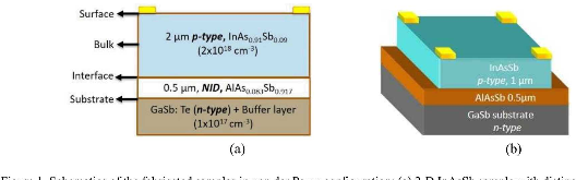 Figure 1: Schematics of the fabricated samples in van der Pauw configuration: (a) 2-D InAsSb sample with distinct conductive paths (b) 3-D etched InAsSb sample.
Works referenced in this record:
Third-generation infrared photodetector arrays
journal, May 2009
- Rogalski, A.; Antoszewski, J.; Faraone, L.
- Journal of Applied Physics, Vol. 105, Issue 9
Identification of dominant recombination mechanisms in narrow-bandgap InAs/InAsSb type-II superlattices and InAsSb alloys
journal, July 2013
- Olson, B. V.; Shaner, E. A.; Kim, J. K.
- Applied Physics Letters, Vol. 103, Issue 5
Evaluation of III–V multilayer transport parameters using quantitative mobility spectrum analysis
journal, February 1997
- Antoszewski, J.; Dell, J. M.; Faraone, L.
- Materials Science and Engineering: B, Vol. 44, Issue 1-3
Ohmic contacts to p-type InAs
journal, September 2006
- Lysczek, E. M.; Robinson, J. A.; Mohney, S. E.
- Materials Science and Engineering: B, Vol. 134, Issue 1
Magneto-transport characterization using quantitative mobility-spectrum analysis
journal, September 1995
- Antoszewski, J.; Seymour, D. J.; Faraone, L.
- Journal of Electronic Materials, Vol. 24, Issue 9
Direct minority carrier transport characterization of InAs/InAsSb superlattice nBn photodetectors
journal, February 2015
- Zuo, Daniel; Liu, Runyu; Wasserman, Daniel
- Applied Physics Letters, Vol. 106, Issue 7
Long-wave infrared nBn photodetectors based on InAs/InAsSb type-II superlattices
journal, October 2012
- Kim, H. S.; Cellek, O. O.; Lin, Zhi-Yuan
- Applied Physics Letters, Vol. 101, Issue 16
Accumulation layer profiles at InAs polar surfaces
journal, December 1997
- Bell, G. R.; Jones, T. S.; McConville, C. F.
- Applied Physics Letters, Vol. 71, Issue 25
Heavy and light hole transport in nominally undoped GaSb substrates
journal, January 2015
- Kala, Hemendra; Umana-Membreno, Gilberto A.; Jolley, Gregory
- Applied Physics Letters, Vol. 106, Issue 3
New material systems for third generation infrared photodetectors
journal, January 2008
- Rogalski, A.
- Opto-Electronics Review, Vol. 16, Issue 4
HgCdTe infrared detector material: history, status and outlook
journal, August 2005
- Rogalski, A.
- Reports on Progress in Physics, Vol. 68, Issue 10
HgCdTe barrier infrared detectors
journal, May 2016
- Kopytko, M.; Rogalski, A.
- Progress in Quantum Electronics, Vol. 47
Significantly improved minority carrier lifetime observed in a long-wavelength infrared III-V type-II superlattice comprised of InAs/InAsSb
journal, December 2011
- Steenbergen, E. H.; Connelly, B. C.; Metcalfe, G. D.
- Applied Physics Letters, Vol. 99, Issue 25
Energy-Gap Variation in Mixed Iii–V Alloys
journal, February 1967
- Thompson, A. G.; Woolley, J. C.
- Canadian Journal of Physics, Vol. 45, Issue 2
Determination of electrical transport properties using a novel magnetic field‐dependent Hall technique
journal, July 1987
- Beck, W. A.; Anderson, J. R.
- Journal of Applied Physics, Vol. 62, Issue 2
Quantitative mobility spectrum analysis of carriers in GaSb/InAs/GaSb superlattice
journal, January 2008
- Chandrasekhar Rao, T. V.; Antoszewski, J.; Rodriguez, J. B.
- Journal of Vacuum Science & Technology B: Microelectronics and Nanometer Structures, Vol. 26, Issue 3
Background and interface electron populations in InAs 0.58 Sb 0.42
journal, February 2015
- Svensson, S. P.; Crowne, F. J.; Hier, H. S.
- Semiconductor Science and Technology, Vol. 30, Issue 3
Vertical minority carrier electron transport in p-type InAs/GaSb type-II superlattices
journal, December 2012
- Umana-Membreno, G. A.; Klein, B.; Kala, H.
- Applied Physics Letters, Vol. 101, Issue 25
Proposal for strained type II superlattice infrared detectors
journal, September 1987
- Smith, D. L.; Mailhiot, C.
- Journal of Applied Physics, Vol. 62, Issue 6
Characterizing Multi-Carrier Devices with Quantitative Mobility Spectrum Analysis and Variable Field Hall Measurements
journal, February 2002
- Du, Gang; Lindemuth, J. R.; Dodrill, B. C.
- Japanese Journal of Applied Physics, Vol. 41, Issue Part 1, No. 2B
Midwavelength Infrared Avalanche Photodiode Using InAs–GaSb Strain Layer Superlattice
journal, November 2007
- Mallick, S.; Banerjee, K.; Ghosh, S.
- IEEE Photonics Technology Letters, Vol. 19, Issue 22
Transport measurements on InAs/GaSb superlattice structures for mid-infrared photodiode
journal, November 2009
- Cervera, C.; Perez, J. P.; Chaghi, R.
- Journal of Physics: Conference Series, Vol. 193
Auger recombination in narrow-gap semiconductor superlattices incorporating antimony
journal, December 2002
- Grein, C. H.; Flatté, M. E.; Olesberg, J. T.
- Journal of Applied Physics, Vol. 92, Issue 12
Characterization of n-Type and p-Type Long-Wave InAs/InAsSb Superlattices
journal, July 2017
- Brown, A. E.; Baril, N.; Zuo, D.
- Journal of Electronic Materials, Vol. 46, Issue 9
Improved quantitative mobility spectrum analysis for Hall characterization
journal, November 1998
- Vurgaftman, I.; Meyer, J. R.; Hoffman, C. A.
- Journal of Applied Physics, Vol. 84, Issue 9
Figures / Tables found in this record: