
Assessing failure in epitaxially encapsulated micro-scale sensors using micro and nano x-ray computed tomography
Abstract
Millions of micro electro mechanical system sensors are fabricated each year using an ultra-clean process that allows for a vacuum-encapsulated cavity. These devices have a multi-layer structure that contains hidden layers with highly doped silicon, which makes common imaging techniques ineffective. Thus, examining device features post-fabrication, and testing, is a significant challenge. Here in this paper, we use a combination of micro- and nano-scale x-ray computed tomography to study device features and assess failure mechanisms in such devices without destroying the ultra-clean cavity. This provides a unique opportunity to examine surfaces and trace failure mechanisms to specific steps in the fabrication process.
- Publication Date:
- Research Org.:
- SLAC National Accelerator Lab., Menlo Park, CA (United States)
- Sponsoring Org.:
- USDOE Office of Science (SC), Basic Energy Sciences (BES); Defense Advanced Research Projects Agency (DARPA)
- OSTI Identifier:
- 1461954
- Grant/Contract Number:
- AC02-76SF00515; N66001-12-1-4260; ECS-9731293
- Resource Type:
- Accepted Manuscript
- Journal Name:
- MRS Communications
- Additional Journal Information:
- Journal Volume: 8; Journal Issue: 02; Journal ID: ISSN 2159-6859
- Publisher:
- Materials Research Society - Cambridge University Press
- Country of Publication:
- United States
- Language:
- English
- Subject:
- 42 ENGINEERING
Citation Formats
                    Comenencia Ortiz, Lizmarie, Heinz, David B., Flader, Ian B., Alter, Anne L., Shin, Dongsuk D., Chen, Yunhan, and Kenny, Thomas W. Assessing failure in epitaxially encapsulated micro-scale sensors using micro and nano x-ray computed tomography.  United States: N. p., 2018.
Web.  doi:10.1557/mrc.2018.70.
Comenencia Ortiz, Lizmarie, Heinz, David B., Flader, Ian B., Alter, Anne L., Shin, Dongsuk D., Chen, Yunhan, & Kenny, Thomas W. Assessing failure in epitaxially encapsulated micro-scale sensors using micro and nano x-ray computed tomography. United States. https://doi.org/10.1557/mrc.2018.70
                    Comenencia Ortiz, Lizmarie, Heinz, David B., Flader, Ian B., Alter, Anne L., Shin, Dongsuk D., Chen, Yunhan, and Kenny, Thomas W. Thu .
"Assessing failure in epitaxially encapsulated micro-scale sensors using micro and nano x-ray computed tomography".  United States.  https://doi.org/10.1557/mrc.2018.70.  https://www.osti.gov/servlets/purl/1461954.
@article{osti_1461954,

  title        = {Assessing failure in epitaxially encapsulated micro-scale sensors using micro and nano x-ray computed tomography},

  author       = {Comenencia Ortiz, Lizmarie and Heinz, David B. and Flader, Ian B. and Alter, Anne L. and Shin, Dongsuk D. and Chen, Yunhan and Kenny, Thomas W.},

  abstractNote = {Millions of micro electro mechanical system sensors are fabricated each year using an ultra-clean process that allows for a vacuum-encapsulated cavity. These devices have a multi-layer structure that contains hidden layers with highly doped silicon, which makes common imaging techniques ineffective. Thus, examining device features post-fabrication, and testing, is a significant challenge. Here in this paper, we use a combination of micro- and nano-scale x-ray computed tomography to study device features and assess failure mechanisms in such devices without destroying the ultra-clean cavity. This provides a unique opportunity to examine surfaces and trace failure mechanisms to specific steps in the fabrication process.},

  doi          = {10.1557/mrc.2018.70},

  journal      = {MRS Communications},

  number       = 02,

  volume       = 8,

  place        = {United States},

  year         = {Thu Apr 12 00:00:00 EDT 2018},

  month        = {Thu Apr 12 00:00:00 EDT 2018}

}
 Search WorldCat to find libraries that may hold this journal
Web of Science
Figures / Tables:
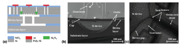 Figure 1: Schematic representation of devices and current imaging techniques used to assess vacuum-sealed structures: (a) schematic representation of cross-section of a die fabricated with the vacuum-sealed encapsulation process, (b) SEM image of cross section of a resonant accelerometer, (c) IR image of an accelerometer with micro-tether.
Works referenced in this record:
High-resolution X-ray imaging—a powerful nondestructive technique for applications in semiconductor industry
journal, May 2008
- Zschech, Ehrenfried; Yun, Wenbing; Schneider, Gerd
- Applied Physics A, Vol. 92, Issue 3
Critical Review: Adhesion in surface micromechanical structures
journal, January 1997
- Maboudian, Roya
- Journal of Vacuum Science & Technology B: Microelectronics and Nanometer Structures, Vol. 15, Issue 1
On the stiction of MEMS materials
journal, June 2005
- Zhuang, Y. X.; Menon, A.
- Tribology Letters, Vol. 19, Issue 2
Experimental Investigation Into Stiction Forces and Dynamic Mechanical Anti-Stiction Solutions in Ultra-Clean Encapsulated MEMS Devices
journal, June 2016
- Heinz, David B.; Hong, Vu A.; Ahn, Chae Hyuck
- Journal of Microelectromechanical Systems, Vol. 25, Issue 3
High-resolution X-ray computed tomography of through silicon vias for RF MEMS integrated passive device applications
journal, August 2015
- de Veen, P. J.; Bos, C.; Hoogstede, D. R.
- Microelectronics Reliability, Vol. 55, Issue 9-10
Frequency stability of wafer-scale film encapsulated silicon based MEMS resonators
journal, May 2007
- Kim, Bongsang; Candler, Rob N.; Hopcroft, Matthew A.
- Sensors and Actuators A: Physical, Vol. 136, Issue 1
TXM-Wizard : a program for advanced data collection and evaluation in full-field transmission X-ray microscopy
journal, January 2012
- Liu, Yijin; Meirer, Florian; Williams, Phillip A.
- Journal of Synchrotron Radiation, Vol. 19, Issue 2
A reaction-layer mechanism for the delayed failure of micron-scale polycrystalline silicon structural films subjected to high-cycle fatigue loading
journal, August 2002
- Muhlstein, C. L.; Stach, E. A.; Ritchie, R. O.
- Acta Materialia, Vol. 50, Issue 14
X-Ray Interactions: Photoabsorption, Scattering, Transmission, and Reflection at E = 50-30,000 eV, Z = 1-92
journal, July 1993
- Henke, B. L.; Gullikson, E. M.; Davis, J. C.
- Atomic Data and Nuclear Data Tables, Vol. 54, Issue 2, p. 181-342
Fatigue Experiments on Single Crystal Silicon in an Oxygen-Free Environment
journal, April 2015
- Hong, Vu A.; Yoneoka, Shingo; Messana, Matthew W.
- Journal of Microelectromechanical Systems, Vol. 24, Issue 2
X-ray metrology for advanced microelectronics
journal, January 2010
- Wyon, C.
- The European Physical Journal Applied Physics, Vol. 49, Issue 2
Long-Term and Accelerated Life Testing of a Novel Single-Wafer Vacuum Encapsulation for MEMS Resonators
journal, January 2006
- Candler, Rob N.; Hopcroft, Matthew A.; Kim, Bongsang
- Journal of Microelectromechanical Systems, Vol. 15, Issue 6
A Unified Epi-Seal Process for Fabrication of High-Stability Microelectromechanical Devices
journal, June 2016
- Yang, Yushi; Ng, Eldwin J.; Chen, Yunhan
- Journal of Microelectromechanical Systems, Vol. 25, Issue 3
Robust Method of Fabricating Epitaxially Encapsulated MEMS Devices with Large Gaps
journal, December 2017
- Chen, Yunhan; Flader, Ian B.; Shin, Dongsuk D.
- Journal of Microelectromechanical Systems, Vol. 26, Issue 6
Figures / Tables found in this record: