
Proton irradiation effects on minority carrier diffusion length and defect introduction in homoepitaxial and heteroepitaxial n-GaN [Proton irradiation effects on minority carrier diffusion length and defect introduction in homoepitaxial n-GaN]
Abstract
Here, inherent advantages of wide bandgap materials make GaN-based devices attractive for power electronics and applications in radiation environments. Recent advances in the availability of wafer-scale, bulk GaN substrates have enabled the production of high quality, low defect density GaN devices, but fundamental studies of carrier transport and radiation hardness in such devices are lacking. Here, we report measurements of the hole diffusion length in low threading dislocation density (TDD), homoepitaxial n-GaN, and high TDD heteroepitaxial n-GaN Schottky diodes before and after irradiation with 2.5 MeV protons at fluences of 4–6 × 10¹³ protons/cm2. We also characterize the specimens before and after irradiation using electron beam-induced-current (EBIC) imaging, cathodoluminescence, deep level optical spectroscopy (DLOS), steady-state photocapacitance, and lighted capacitance-voltage (LCV) techniques. We observe a substantial reduction in the hole diffusion length following irradiation (50%–55%) and the introduction of electrically active defects which could be attributed to gallium vacancies and associated complexes (VGa-related), carbon impurities (C-related), and gallium interstitials (Gai). EBIC imaging suggests long-range migration and clustering of radiation-induced point defects over distances of ~500 nm, which suggests mobile Gai. Following irradiation, DLOS and LCV reveal the introduction of a prominent optical energy level at 1.9 eV below the conduction bandmore »
- Authors:
-
- Sandia National Lab. (SNL-CA), Livermore, CA (United States)
- Sandia National Lab. (SNL-NM), Albuquerque, NM (United States)
- Publication Date:
- Research Org.:
- Sandia National Lab. (SNL-NM), Albuquerque, NM (United States)
- Sponsoring Org.:
- USDOE National Nuclear Security Administration (NNSA)
- OSTI Identifier:
- 1421641
- Alternate Identifier(s):
- OSTI ID: 1414507; OSTI ID: 1872015
- Report Number(s):
- SAND-2017-13818J; SAND2022-5388J
Journal ID: ISSN 0021-8979; 659684; TRN: US1801537
- Grant/Contract Number:
- AC04-94AL85000; NA0003525
- Resource Type:
- Accepted Manuscript
- Journal Name:
- Journal of Applied Physics
- Additional Journal Information:
- Journal Volume: 122; Journal Issue: 23; Journal ID: ISSN 0021-8979
- Publisher:
- American Institute of Physics (AIP)
- Country of Publication:
- United States
- Language:
- English
- Subject:
- 72 PHYSICS OF ELEMENTARY PARTICLES AND FIELDS
Citation Formats
                    Collins, K. C., Armstrong, Andrew M., Allerman, Andrew A., Vizkelethy, G., Van Deusen, Stuart B., Leonard, Francois, and Talin, Albert Alec. Proton irradiation effects on minority carrier diffusion length and defect introduction in homoepitaxial and heteroepitaxial n-GaN [Proton irradiation effects on minority carrier diffusion length and defect introduction in homoepitaxial n-GaN].  United States: N. p., 2017.
Web.  doi:10.1063/1.5006814.
Collins, K. C., Armstrong, Andrew M., Allerman, Andrew A., Vizkelethy, G., Van Deusen, Stuart B., Leonard, Francois, & Talin, Albert Alec. Proton irradiation effects on minority carrier diffusion length and defect introduction in homoepitaxial and heteroepitaxial n-GaN [Proton irradiation effects on minority carrier diffusion length and defect introduction in homoepitaxial n-GaN]. United States. https://doi.org/10.1063/1.5006814
                    Collins, K. C., Armstrong, Andrew M., Allerman, Andrew A., Vizkelethy, G., Van Deusen, Stuart B., Leonard, Francois, and Talin, Albert Alec. Thu .
"Proton irradiation effects on minority carrier diffusion length and defect introduction in homoepitaxial and heteroepitaxial n-GaN [Proton irradiation effects on minority carrier diffusion length and defect introduction in homoepitaxial n-GaN]".  United States.  https://doi.org/10.1063/1.5006814.  https://www.osti.gov/servlets/purl/1421641.
@article{osti_1421641,

  title        = {Proton irradiation effects on minority carrier diffusion length and defect introduction in homoepitaxial and heteroepitaxial n-GaN [Proton irradiation effects on minority carrier diffusion length and defect introduction in homoepitaxial n-GaN]},

  author       = {Collins, K. C. and Armstrong, Andrew M. and Allerman, Andrew A. and Vizkelethy, G. and Van Deusen, Stuart B. and Leonard, Francois and Talin, Albert Alec},

  abstractNote = {Here, inherent advantages of wide bandgap materials make GaN-based devices attractive for power electronics and applications in radiation environments. Recent advances in the availability of wafer-scale, bulk GaN substrates have enabled the production of high quality, low defect density GaN devices, but fundamental studies of carrier transport and radiation hardness in such devices are lacking. Here, we report measurements of the hole diffusion length in low threading dislocation density (TDD), homoepitaxial n-GaN, and high TDD heteroepitaxial n-GaN Schottky diodes before and after irradiation with 2.5 MeV protons at fluences of 4–6 × 10¹³ protons/cm2. We also characterize the specimens before and after irradiation using electron beam-induced-current (EBIC) imaging, cathodoluminescence, deep level optical spectroscopy (DLOS), steady-state photocapacitance, and lighted capacitance-voltage (LCV) techniques. We observe a substantial reduction in the hole diffusion length following irradiation (50%–55%) and the introduction of electrically active defects which could be attributed to gallium vacancies and associated complexes (VGa-related), carbon impurities (C-related), and gallium interstitials (Gai). EBIC imaging suggests long-range migration and clustering of radiation-induced point defects over distances of ~500 nm, which suggests mobile Gai. Following irradiation, DLOS and LCV reveal the introduction of a prominent optical energy level at 1.9 eV below the conduction band edge, consistent with the introduction of Gai.},

  doi          = {10.1063/1.5006814},

  journal      = {Journal of Applied Physics},

  number       = 23,

  volume       = 122,

  place        = {United States},

  year         = {Thu Dec 21 00:00:00 EST 2017},

  month        = {Thu Dec 21 00:00:00 EST 2017}

}
 Search WorldCat to find libraries that may hold this journal
Web of Science
Figures / Tables:
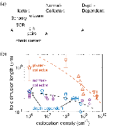 FIG. 1: (a) Schematic of the three EBIC configurations used for measuring minority carrier diffusion length. (b) Reported values for hole diffusion length in unirradiated n-GaN vs dislocation density, acquired using the planar-collector (red), normal collector (purple), or depth-dependent (blue) configurations. Measurements from this work on unirradiated GaN with lowmore »
Works referenced in this record:
Dislocation reduction in GaN crystal by advanced-DEEP
journal, July 2007
- Motoki, Kensaku; Okahisa, Takuji; Hirota, Ryu
- Journal of Crystal Growth, Vol. 305, Issue 2
Application of CL/EBIC-SEM Techniques for Characterization of Radiation Effects in Multijunction Solar Cells
journal, December 2010
- Maximenko, S. I.; Messenger, S. R.; Cress, C. D.
- IEEE Transactions on Nuclear Science
Preparation of Large Freestanding GaN Substrates by Hydride Vapor Phase Epitaxy Using GaAs as a Starting Substrate
journal, February 2001
- Motoki, Kensaku; Okahisa, Takuji; Matsumoto, Naoki
- Japanese Journal of Applied Physics, Vol. 40, Issue Part 2, No. 2B
Time-resolved luminescence studies of proton-implanted GaN
journal, September 2009
- Pinos, A.; Marcinkevičius, S.; Usman, M.
- Applied Physics Letters, Vol. 95, Issue 11
First-principles calculations for defects and impurities: Applications to III-nitrides
journal, April 2004
- Van de Walle, Chris G.; Neugebauer, Jörg
- Journal of Applied Physics, Vol. 95, Issue 8
Bulk GaN crystals grown by HVPE
journal, May 2009
- Fujito, Kenji; Kubo, Shuichi; Nagaoka, Hirobumi
- Journal of Crystal Growth, Vol. 311, Issue 10
Recombination Properties of Defects in Gallium Nitride
journal, April 2001
- Castaldini, Antonio; Cavallini, Anna; Polenta, L.
- Solid State Phenomena, Vol. 78-79
The values of minority carrier diffusion lengths and lifetimes in GaN and their implications for bipolar devices
journal, February 2000
- Bandić, Z. Z.; Bridger, P. M.; Piquette, E. C.
- Solid-State Electronics, Vol. 44, Issue 2
What is the real value of diffusion length in GaN?
journal, April 2015
- Yakimov, E. B.
- Journal of Alloys and Compounds, Vol. 627
Effects of proton implantation on electrical and recombination properties of n-GaN
journal, November 2000
- Polyakov, A. Y.; Usikov, A. S.; Theys, B.
- Solid-State Electronics, Vol. 44, Issue 11
Impact of substrate temperature on the incorporation of carbon-related defects and mechanism for semi-insulating behavior in GaN grown by molecular beam epitaxy
journal, February 2006
- Armstrong, A.; Poblenz, C.; Green, D. S.
- Applied Physics Letters, Vol. 88, Issue 8
Electrical, optical, and structural properties of GaN films prepared by hydride vapor phase epitaxy
journal, December 2014
- Polyakov, A. Y.; Smirnov, N. B.; Yakimov, E. B.
- Journal of Alloys and Compounds, Vol. 617
Depth dependence of defect density and stress in GaN grown on SiC
journal, December 2005
- Faleev, N.; Temkin, H.; Ahmad, I.
- Journal of Applied Physics, Vol. 98, Issue 12
Impact of proton irradiation on deep level states in n-GaN
journal, July 2013
- Zhang, Z.; Arehart, A. R.; Cinkilic, E.
- Applied Physics Letters, Vol. 103, Issue 4
Donor nonuniformity in undoped and Si doped n-GaN prepared by epitaxial lateral overgrowth
journal, January 2008
- Yakimov, E. B.; Vergeles, P. S.; Polyakov, A. Y.
- Applied Physics Letters, Vol. 92, Issue 4
Power semiconductor device figure of merit for high-frequency applications
journal, October 1989
- Baliga, B. J.
- IEEE Electron Device Letters, Vol. 10, Issue 10
SRIM – The stopping and range of ions in matter (2010)
journal, June 2010
- Ziegler, James F.; Ziegler, M. D.; Biersack, J. P.
- Nuclear Instruments and Methods in Physics Research Section B: Beam Interactions with Materials and Atoms, Vol. 268, Issue 11-12
Luminescence properties of defects in GaN
journal, March 2005
- Reshchikov, Michael A.; Morkoç, Hadis
- Journal of Applied Physics, Vol. 97, Issue 6
Review—Ionizing Radiation Damage Effects on GaN Devices
journal, November 2015
- Pearton, S. J.; Ren, F.; Patrick, Erin
- ECS Journal of Solid State Science and Technology, Vol. 5, Issue 2
Nitrogen Effusion and Self-Diffusion in Ga 14 N/Ga 15 N Isotope Heterostructures
journal, May 1998
- Ambacher, Oliver; Freudenberg, Frank; Dimitrov, Roman
- Japanese Journal of Applied Physics, Vol. 37, Issue Part 1, No. 5A
CASINO V2.42—A Fast and Easy-to-use Modeling Tool for Scanning Electron Microscopy and Microanalysis Users
journal, January 2007
- Drouin, Dominique; Couture, Alexandre Réal; Joly, Dany
- Scanning, Vol. 29, Issue 3
Imaging the Impact of Proton Irradiation on Edge Terminations in Vertical GaN PIN Diodes
journal, July 2017
- Collins, K. C.; King, M. P.; Dickerson, J. R.
- IEEE Electron Device Letters, Vol. 38, Issue 7
Displacement Damage Evolution in GaAs Following Electron, Proton and Silicon Ion Irradiation
journal, December 2007
- Warner, Jeffrey H.; Messenger, Scott R.; Walters, Robert J.
- IEEE Transactions on Nuclear Science, Vol. 54, Issue 6
A method to determine deep level profiles in highly compensated, wide band gap semiconductors
journal, April 2005
- Armstrong, A.; Arehart, A. R.; Ringel, S. A.
- Journal of Applied Physics, Vol. 97, Issue 8
Photoionization cross-section analysis for a deep trap contributing to current collapse in GaN field-effect transistors
journal, July 2004
- Pässler, Roland
- Journal of Applied Physics, Vol. 96, Issue 1
EBIC measurements of small diffusion length in semiconductor structures
journal, April 2007
- Yakimov, E. B.; Borisov, S. S.; Zaitsev, S. I.
- Semiconductors, Vol. 41, Issue 4
Minority carrier diffusion length in GaN: Dislocation density and doping concentration dependence
journal, January 2005
- Kumakura, K.; Makimoto, T.; Kobayashi, N.
- Applied Physics Letters, Vol. 86, Issue 5
Proton implantation effects on electrical and luminescent properties of p-GaN
journal, September 2003
- Polyakov, A. Y.; Smirnov, N. B.; Govorkov, A. V.
- Journal of Applied Physics, Vol. 94, Issue 5
Gallium nitride devices for power electronic applications
journal, June 2013
- Baliga, B. Jayant
- Semiconductor Science and Technology, Vol. 28, Issue 7
Critical issues for homoepitaxial GaN growth by molecular beam epitaxy on hydride vapor-phase epitaxy-grown GaN substrates
journal, December 2016
- Storm, D. F.; Hardy, M. T.; Katzer, D. S.
- Journal of Crystal Growth, Vol. 456
Electron beam and optical depth profiling of quasibulk GaN
journal, October 2000
- Chernyak, L.; Osinsky, A.; Nootz, G.
- Applied Physics Letters, Vol. 77, Issue 17
Diffusivity of native defects in GaN
journal, January 2004
- Limpijumnong, Sukit; Van de Walle, Chris
- Physical Review B, Vol. 69, Issue 3
Bulk GaN crystals grown by HVPE
journal, May 2009
- Fujito, Kenji; Kubo, Shuichi; Nagaoka, Hirobumi
- Journal of Crystal Growth, Vol. 311, Issue 10
Detection of Interstitial Ga in GaN
journal, September 2000
- Chow, K. H.; Watkins, G. D.; Usui, Akira
- Physical Review Letters, Vol. 85, Issue 13
Non-Specific Streptolysin o Inhibition in Diseases of the Liver and Biliary System
journal, August 2009
- Hällén, J.
- Acta Pathologica Microbiologica Scandinavica, Vol. 57, Issue 3
Mechanism of Yellow Luminescence in GaN
journal, December 1980
- Ogino, Toshio; Aoki, Masaharu
- Japanese Journal of Applied Physics, Vol. 19, Issue 12
Works referencing / citing this record:
Optimal Semiconductors for 3H and 63Ni Betavoltaics
journal, July 2019
- Maximenko, Sergey I.; Moore, Jim E.; Affouda, Chaffra A.
- Scientific Reports, Vol. 9, Issue 1
Design considerations for three-dimensional betavoltaics
journal, June 2019
- Murphy, John W.; Voss, Lars F.; Frye, Clint D.
- AIP Advances, Vol. 9, Issue 6
Investigation of dry-etch-induced defects in >600 V regrown, vertical, GaN, p-n diodes using deep-level optical spectroscopy
journal, October 2019
- Pickrell, G. W.; Armstrong, A. M.; Allerman, A. A.
- Journal of Applied Physics, Vol. 126, Issue 14
Modeling dislocation-related leakage currents in GaN p-n diodes
journal, December 2019
- Robertson, C. A.; Qwah, K. S.; Wu, Y. -R.
- Journal of Applied Physics, Vol. 126, Issue 24
Figures / Tables found in this record: