Office of Scientific and Technical Information
Photocarrier generation from interlayer charge-transfer transitions in WS2-graphene heterostructures
Abstract
Efficient interfacial carrier generation in van der Waals heterostructures is critical for their electronic and optoelectronic applications. We demonstrate broadband photocarrier generation in WS2-graphene heterostructures by imaging interlayer coupling–dependent charge generation using ultrafast transient absorption microscopy. Interlayer charge-transfer (CT) transitions and hot carrier injection from graphene allow carrier generation by excitation as low as 0.8 eV below the WS2 bandgap. The experimentally determined interlayer CT transition energies are consistent with those predicted from the first-principles band structure calculation. CT interactions also lead to additional carrier generation in the visible spectral range in the heterostructures compared to that in the single-layer WS2 alone. The lifetime of the charge-separated states is measured to be ~1 ps. These results suggest that interlayer interactions make graphene–two-dimensional semiconductor heterostructures very attractive for photovoltaic and photodetector applications because of the combined benefits of high carrier mobility and enhanced broadband photocarrier generation.
- Authors:
-
 [1];
[1];
[2];
[1];
[1];
[2];
[1]
[1];
[1];
[2];
[1];
[1];
[2];
[1]
- Purdue Univ., West Lafayette, IN (United States)
- Universität Leipzig (Germany); Jacobs University Bremen (Germany)
- Publication Date:
- Research Org.:
- Purdue Univ., West Lafayette, IN (United States)
- Sponsoring Org.:
- USDOE Office of Science (SC), Basic Energy Sciences (BES)
- OSTI Identifier:
- 1499923
- Grant/Contract Number:
- SC0016356
- Resource Type:
- Journal Article: Accepted Manuscript
- Journal Name:
- Science Advances
- Additional Journal Information:
- Journal Volume: 4; Journal Issue: 2; Journal ID: ISSN 2375-2548
- Publisher:
- AAAS
- Country of Publication:
- United States
- Language:
- English
- Subject:
- 36 MATERIALS SCIENCE
Citation Formats
                    Yuan, Long, Chung, Ting-Fung, Kuc, Agnieszka, Wan, Yan, Xu, Yang, Chen, Yong P., Heine, Thomas, and Huang, Libai. Photocarrier generation from interlayer charge-transfer transitions in WS2-graphene heterostructures.  United States: N. p., 2018.
        Web.  doi:10.1126/sciadv.1700324.
Yuan, Long, Chung, Ting-Fung, Kuc, Agnieszka, Wan, Yan, Xu, Yang, Chen, Yong P., Heine, Thomas, & Huang, Libai. Photocarrier generation from interlayer charge-transfer transitions in WS2-graphene heterostructures. United States. https://doi.org/10.1126/sciadv.1700324
                    Yuan, Long, Chung, Ting-Fung, Kuc, Agnieszka, Wan, Yan, Xu, Yang, Chen, Yong P., Heine, Thomas, and Huang, Libai. 2018.
        "Photocarrier generation from interlayer charge-transfer transitions in WS2-graphene heterostructures".  United States.  https://doi.org/10.1126/sciadv.1700324.  https://www.osti.gov/servlets/purl/1499923.
@article{osti_1499923,

  title        = {Photocarrier generation from interlayer charge-transfer transitions in WS2-graphene heterostructures},

  author       = {Yuan, Long and Chung, Ting-Fung and Kuc, Agnieszka and Wan, Yan and Xu, Yang and Chen, Yong P. and Heine, Thomas and Huang, Libai},

  abstractNote = {Efficient interfacial carrier generation in van der Waals heterostructures is critical for their electronic and optoelectronic applications. We demonstrate broadband photocarrier generation in WS2-graphene heterostructures by imaging interlayer coupling–dependent charge generation using ultrafast transient absorption microscopy. Interlayer charge-transfer (CT) transitions and hot carrier injection from graphene allow carrier generation by excitation as low as 0.8 eV below the WS2 bandgap. The experimentally determined interlayer CT transition energies are consistent with those predicted from the first-principles band structure calculation. CT interactions also lead to additional carrier generation in the visible spectral range in the heterostructures compared to that in the single-layer WS2 alone. The lifetime of the charge-separated states is measured to be ~1 ps. These results suggest that interlayer interactions make graphene–two-dimensional semiconductor heterostructures very attractive for photovoltaic and photodetector applications because of the combined benefits of high carrier mobility and enhanced broadband photocarrier generation.},

  doi          = {10.1126/sciadv.1700324},

  url          = {https://www.osti.gov/biblio/1499923},
  journal      = {Science Advances},

  issn         = {2375-2548},

  number       = 2,

  volume       = 4,

  place        = {United States},

  year         = {Fri Feb 02 00:00:00 EST 2018},

  month        = {Fri Feb 02 00:00:00 EST 2018}

}
Web of Science
Figures / Tables:
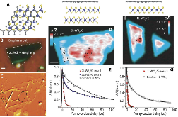 Fig. 1.: Interlayer coupling–dependent charge transfer from WS2 to graphene. (A) Atomicmodels of 1L-WS2/G and 2L-WS2/G interfaces, with aligned layers. (B) Optical image of the 2L-WS2/G heterostructure. (C) AFM height image of the 2L-WS2/G heterostructure. (D) Correlated TAM image of the 2L-WS2/G heterostructure measured at 0 ps probing the A-excitonmore »
Works referenced in this record:
Generalized Gradient Approximation Made Simple
journal, October 1996
- Perdew, John P.; Burke, Kieron; Ernzerhof, Matthias
- Physical Review Letters, Vol. 77, Issue 18, p. 3865-3868
Ultrafast Spatial Imaging of Charge Dynamics in Heterogeneous Polymer Blends
journal, March 2012
- Wong, Chris Tsz On; Lo, Shun Shang; Huang, Libai
- The Journal of Physical Chemistry Letters, Vol. 3, Issue 7
Photodetectors based on graphene, other two-dimensional materials and hybrid systems
journal, October 2014
- Koppens, F. H. L.; Mueller, T.; Avouris, Ph.
- Nature Nanotechnology, Vol. 9, Issue 10
Projector augmented-wave method
journal, December 1994
- Blöchl, P. E.
- Physical Review B, Vol. 50, Issue 24, p. 17953-17979
Hybrid functionals based on a screened Coulomb potential
journal, May 2003
- Heyd, Jochen; Scuseria, Gustavo E.; Ernzerhof, Matthias
- The Journal of Chemical Physics, Vol. 118, Issue 18
Hybrid Graphene and Graphitic Carbon Nitride Nanocomposite: Gap Opening, Electron–Hole Puddle, Interfacial Charge Transfer, and Enhanced Visible Light Response
journal, February 2012
- Du, Aijun; Sanvito, Stefano; Li, Zhen
- Journal of the American Chemical Society, Vol. 134, Issue 9
Scaling of Excitons in Carbon Nanotubes
journal, June 2004
- Perebeinos, Vasili; Tersoff, J.; Avouris, Phaedon
- Physical Review Letters, Vol. 92, Issue 25
Probing Interlayer Interactions in Transition Metal Dichalcogenide Heterostructures by Optical Spectroscopy: MoS 2 /WS 2 and MoSe 2 /WSe 2
journal, July 2015
- Rigosi, Albert F.; Hill, Heather M.; Li, Yilei
- Nano Letters, Vol. 15, Issue 8
Electron transfer and coupling in graphene–tungsten disulfide van der Waals heterostructures
journal, November 2014
- He, Jiaqi; Kumar, Nardeep; Bellus, Matthew Z.
- Nature Communications, Vol. 5, Issue 1
Energy Transfer from Quantum Dots to Graphene and MoS 2 : The Role of Absorption and Screening in Two-Dimensional Materials
journal, March 2016
- Raja, Archana; Montoya−Castillo, Andrés; Zultak, Johanna
- Nano Letters, Vol. 16, Issue 4
From ultrasoft pseudopotentials to the projector augmented-wave method
journal, January 1999
- Kresse, G.; Joubert, D.
- Physical Review B, Vol. 59, Issue 3, p. 1758-1775
Optical separation of mechanical strain from charge doping in graphene
journal, January 2012
- Lee, Ji Eun; Ahn, Gwanghyun; Shim, Jihye
- Nature Communications, Vol. 3, Issue 1
Vertical Heterostructure of Two-Dimensional MoS 2 and WSe 2 with Vertically Aligned Layers
journal, January 2015
- Yu, Jung Ho; Lee, Hye Ryoung; Hong, Seung Sae
- Nano Letters, Vol. 15, Issue 2
Quantum Coherence Facilitates Efficient Charge Separation at a MoS 2 /MoSe 2 van der Waals Junction
journal, February 2016
- Long, Run; Prezhdo, Oleg V.
- Nano Letters, Vol. 16, Issue 3
Atomically Thin A New Direct-Gap Semiconductor
journal, September 2010
- Mak, Kin Fai; Lee, Changgu; Hone, James
- Physical Review Letters, Vol. 105, Issue 13, Article No.136805
Tuning the electronic structure of monolayer graphene/ van der Waals heterostructures via interlayer twist
journal, November 2015
- Jin, Wencan; Yeh, Po-Chun; Zaki, Nader
- Physical Review B, Vol. 92, Issue 20
Electric Field Effect Tuning of Electron-Phonon Coupling in Graphene
journal, April 2007
- Yan, Jun; Zhang, Yuanbo; Kim, Philip
- Physical Review Letters, Vol. 98, Issue 16
An ab Initio Hartree−Fock Study of the Cubic and Tetragonal Phases of Bulk Tungsten Trioxide
journal, January 1996
- Corà, Furio; Patel, Atul; Harrison, Nicholas M.
- Journal of the American Chemical Society, Vol. 118, Issue 48
Interlayer Exciton Optoelectronics in a 2D Heterostructure p–n Junction
journal, January 2017
- Ross, Jason S.; Rivera, Pasqual; Schaibley, John
- Nano Letters, Vol. 17, Issue 2
Giant bandgap renormalization and excitonic effects in a monolayer transition metal dichalcogenide semiconductor
journal, August 2014
- Ugeda, Miguel M.; Bradley, Aaron J.; Shi, Su-Fei
- Nature Materials, Vol. 13, Issue 12
Two-dimensional gas of massless Dirac fermions in graphene
journal, November 2005
- Novoselov, K. S.; Geim, A. K.; Morozov, S. V.
- Nature, Vol. 438, Issue 7065, p. 197-200
Vertical 2D Heterostructures
journal, July 2015
- Lotsch, Bettina V.
- Annual Review of Materials Research, Vol. 45, Issue 1
Light-emitting diodes by band-structure engineering in van der Waals heterostructures
journal, February 2015
- Withers, F.; Del Pozo-Zamudio, O.; Mishchenko, A.
- Nature Materials, Vol. 14, Issue 3
Ultrafast Carrier Dynamics in Graphite
journal, February 2009
- Breusing, Markus; Ropers, Claus; Elsaesser, Thomas
- Physical Review Letters, Vol. 102, Issue 8
Exciton broadening in WS2 /graphene heterostructures
text, January 2017
- Hill, Heather M.; Rigosi, Albert F.; Raja, Archana
- Universität Regensburg
Coulomb engineering of the bandgap and excitons in two-dimensional materials
text, January 2017
- Raja, Archana; Chaves, Andrey; Yu, Jaeeun
- Universität Regensburg
Photo-thermionic effect in vertical graphene heterostructures
journal, July 2016
- Massicotte, M.; Schmidt, P.; Vialla, F.
- Nature Communications, Vol. 7, Issue 1
Strong Light-Matter Interactions in Heterostructures of Atomically Thin Films
journal, May 2013
- Britnell, L.; Ribeiro, R. M.; Eckmann, A.
- Science, Vol. 340, Issue 6138
Electronic structure of AlFeN films exhibiting crystallographic orientation change from c- to a-axis with Fe concentrations and annealing effect
journal, February 2020
- Tatemizo, Nobuyuki; Imada, Saki; Okahara, Kizuna
- Scientific Reports, Vol. 10, Issue 1
Interlayer Coupling in Twisted WSe 2 /WS 2 Bilayer Heterostructures Revealed by Optical Spectroscopy
journal, June 2016
- Wang, Kai; Huang, Bing; Tian, Mengkun
- ACS Nano, Vol. 10, Issue 7
Efficient iterative schemes for ab initio total-energy calculations using a plane-wave basis set
journal, October 1996
- Kresse, G.; Furthmüller, J.
- Physical Review B, Vol. 54, Issue 16, p. 11169-11186
Semiconducting Monolayer Materials as a Tunable Platform for Excitonic Solar Cells
journal, October 2012
- Bernardi, Marco; Palummo, Maurizia; Grossman, Jeffrey C.
- ACS Nano, Vol. 6, Issue 11
Direct Observation of Interlayer Hybridization and Dirac Relativistic Carriers in Graphene/MoS 2 van der Waals Heterostructures
journal, January 2015
- Coy Diaz, Horacio; Avila, José; Chen, Chaoyu
- Nano Letters, Vol. 15, Issue 2
Electronic properties of single-layer tungsten disulfide on epitaxial graphene on silicon carbide
journal, January 2017
- Forti, Stiven; Rossi, Antonio; Büch, Holger
- Nanoscale, Vol. 9, Issue 42
Equally Efficient Interlayer Exciton Relaxation and Improved Absorption in Epitaxial and Nonepitaxial MoS 2 /WS 2 Heterostructures
journal, December 2014
- Yu, Yifei; Hu, Shi; Su, Liqin
- Nano Letters, Vol. 15, Issue 1
Semiempirical GGA-type density functional constructed with a long-range dispersion correction
journal, January 2006
- Grimme, Stefan
- Journal of Computational Chemistry, Vol. 27, Issue 15, p. 1787-1799
Reducing Dzyaloshinskii-Moriya interaction and field-free spin-orbit torque switching in synthetic antiferromagnets
journal, May 2021
- Chen, Ruyi; Cui, Qirui; Liao, Liyang
- Nature Communications, Vol. 12, Issue 1
Coulomb engineering of the bandgap and excitons in two-dimensional materials
text, January 2017
- Chernikov, Alexey; Raja, Archana; Chaves, Andrey
- Universität Regensburg
Highly efficient gate-tunable photocurrent generation in vertical heterostructures of layered materials
journal, October 2013
- Yu, Woo Jong; Liu, Yuan; Zhou, Hailong
- Nature Nanotechnology, Vol. 8, Issue 12
Ground-State Depletion Microscopy: Detection Sensitivity of Single-Molecule Optical Absorption at Room Temperature
journal, November 2010
- Chong, Shasha; Min, Wei; Xie, X. Sunney
- The Journal of Physical Chemistry Letters, Vol. 1, Issue 23
Interlayer orientation-dependent light absorption and emission in monolayer semiconductor stacks
journal, June 2015
- Heo, Hoseok; Sung, Ji Ho; Cha, Soonyoung
- Nature Communications, Vol. 6, Issue 1
Synthetic Graphene Grown by Chemical Vapor Deposition on Copper Foils
journal, April 2013
- Chung, Ting Fung; Shen, Tian; Cao, Helin
- International Journal of Modern Physics B, Vol. 27, Issue 10
Static lattice and electron properties of (magnesite) calculated by ab initio periodic Hartree-Fock methods
journal, April 1993
- Catti, M.; Pavese, A.; Dovesi, R.
- Physical Review B, Vol. 47, Issue 15
Quantum Mechnical Hartree-Fock Study of the Elastic Properties of Li2S and Na2S
journal, May 1993
- Lichanot, A.; Aprà, E.; Dovesi, R.
- physica status solidi (b), Vol. 177, Issue 1
Observation of Exciton Redshift–Blueshift Crossover in Monolayer WS 2
journal, June 2017
- Sie, E. J.; Steinhoff, A.; Gies, C.
- Nano Letters, Vol. 17, Issue 7
Experimental observation of two massless Dirac-fermion gases in graphene-topological insulator heterostructure
journal, May 2016
- Bian, Guang; Chung, Ting-Fung; Chen, Chaoyu
- 2D Materials, Vol. 3, Issue 2
Emerging Photoluminescence in Monolayer MoS2
journal, April 2010
- Splendiani, Andrea; Sun, Liang; Zhang, Yuanbo
- Nano Letters, Vol. 10, Issue 4, p. 1271-1275
Electronic transport in graphene-based heterostructures
journal, May 2014
- Tan, J. Y.; Avsar, A.; Balakrishnan, J.
- Applied Physics Letters, Vol. 104, Issue 18
Tuning Interlayer Coupling in Large-Area Heterostructures with CVD-Grown MoS 2 and WS 2 Monolayers
journal, May 2014
- Tongay, Sefaattin; Fan, Wen; Kang, Jun
- Nano Letters, Vol. 14, Issue 6
Efficient hot-electron transfer by a plasmon-induced interfacial charge-transfer transition
journal, August 2015
- Wu, K.; Chen, J.; McBride, J. R.
- Science, Vol. 349, Issue 6248
Population inversion and giant bandgap renormalization in atomically thin WS2 layers
journal, June 2015
- Chernikov, Alexey; Ruppert, Claudia; Hill, Heather M.
- Nature Photonics, Vol. 9, Issue 7
Graphene: Status and Prospects
journal, June 2009
- Geim, A. K.
- Science, Vol. 324, Issue 5934, p. 1530-1534
Generation of photovoltage in graphene on a femtosecond timescale through efficient carrier heating
journal, April 2015
- Tielrooij, K. J.; Piatkowski, L.; Massicotte, M.
- Nature Nanotechnology, Vol. 10, Issue 5
Picosecond photoresponse in van der Waals heterostructures
journal, October 2015
- Massicotte, M.; Schmidt, P.; Vialla, F.
- Nature Nanotechnology, Vol. 11, Issue 1
Coulomb engineering of the bandgap and excitons in two-dimensional materials
journal, May 2017
- Raja, Archana; Chaves, Andrey; Yu, Jaeeun
- Nature Communications, Vol. 8, Issue 1
Interfacial Charge Transfer Circumventing Momentum Mismatch at Two-Dimensional van der Waals Heterojunctions
journal, May 2017
- Zhu, Haiming; Wang, Jue; Gong, Zizhou
- Nano Letters, Vol. 17, Issue 6
Chemical Vapor Deposition-Derived Graphene with Electrical Performance of Exfoliated Graphene
journal, May 2012
- Petrone, Nicholas; Dean, Cory R.; Meric, Inanc
- Nano Letters, Vol. 12, Issue 6
Evidence for Fast Interlayer Energy Transfer in MoSe 2 /WS 2 Heterostructures
journal, June 2016
- Kozawa, Daichi; Carvalho, Alexandra; Verzhbitskiy, Ivan
- Nano Letters, Vol. 16, Issue 7
Exciton dynamics and annihilation in WS 2 2D semiconductors
journal, January 2015
- Yuan, Long; Huang, Libai
- Nanoscale, Vol. 7, Issue 16
Seeing Many-Body Effects in Single- and Few-Layer Graphene: Observation of Two-Dimensional Saddle-Point Excitons
journal, January 2011
- Mak, Kin Fai; Shan, Jie; Heinz, Tony F.
- Physical Review Letters, Vol. 106, Issue 4
Quasiparticle band-edge energy and band offsets of monolayer of molybdenum and tungsten chalcogenides
journal, July 2013
- Liang, Yufeng; Huang, Shouting; Soklaski, Ryan
- Applied Physics Letters, Vol. 103, Issue 4
Charge Transfer Excitons at van der Waals Interfaces
journal, June 2015
- Zhu, Xiaoyang; Monahan, Nicholas R.; Gong, Zizhou
- Journal of the American Chemical Society, Vol. 137, Issue 26
Heterojunctions in 2D semiconductors: A perfect match
journal, December 2014
- Duesberg, Georg S.
- Nature Materials, Vol. 13, Issue 12, p. 1075-1076
Two-dimensional crystals-based heterostructures: materials with tailored properties
journal, January 2012
- Novoselov, K. S.; Castro Neto, A. H.
- Physica Scripta, Vol. T146
Epitaxial growth of a monolayer WSe2-MoS2 lateral p-n junction with an atomically sharp interface
journal, July 2015
- Li, M. -Y.; Shi, Y.; Cheng, C. -C.
- Science, Vol. 349, Issue 6247
Van der Waals heterostructures
journal, July 2013
- Geim, A. K.; Grigorieva, I. V.
- Nature, Vol. 499, Issue 7459, p. 419-425
Emerging Device Applications for Semiconducting Two-Dimensional Transition Metal Dichalcogenides
journal, January 2014
- Jariwala, Deep; Sangwan, Vinod K.; Lauhon, Lincoln J.
- ACS Nano, Vol. 8, Issue 2
Photo-Induced Bandgap Renormalization Governs the Ultrafast Response of Single-Layer MoS 2
journal, December 2015
- Pogna, Eva A. A.; Marsili, Margherita; De Fazio, Domenico
- ACS Nano, Vol. 10, Issue 1
Two-dimensional atomic crystals
journal, July 2005
- Novoselov, K. S.; Jiang, D.; Schedin, F.
- Proceedings of the National Academy of Sciences, Vol. 102, Issue 30, p. 10451-10453
Ultrafast charge transfer in atomically thin MoS2/WS2 heterostructures
journal, August 2014
- Hong, Xiaoping; Kim, Jonghwan; Shi, Su-Fei
- Nature Nanotechnology, Vol. 9, Issue 9
Effect of compression on the electronic, optical and transport properties of MoS 2 /graphene-based junctions
journal, April 2016
- Ghorbani-Asl, Mahdi; Bristowe, Paul D.; Koziol, K.
- 2D Materials, Vol. 3, Issue 2
Photo-Induced Bandgap Renormalization Governs the Ultrafast Response of Single-Layer MoS2.
journalarticle, January 2016
- Pogna, Eva AA; Marsili, Margherita; De Fazio, Domenico
- American Chemical Society (ACS)
Exciton Binding Energy and Nonhydrogenic Rydberg Series in Monolayer
journal, August 2014
- Chernikov, Alexey; Berkelbach, Timothy C.; Hill, Heather M.
- Physical Review Letters, Vol. 113, Issue 7
Van der Waals metal-semiconductor junction: Weak Fermi level pinning enables effective tuning of Schottky barrier
journal, April 2016
- Liu, Yuanyue; Stradins, Paul; Wei, Su-Huai
- Science Advances, Vol. 2, Issue 4
Observation of long-lived interlayer excitons in monolayer MoSe2–WSe2 heterostructures
journal, February 2015
- Rivera, Pasqual; Schaibley, John R.; Jones, Aaron M.
- Nature Communications, Vol. 6, Issue 1
Graphene photonics and optoelectronics
journal, August 2010
- Bonaccorso, F.; Sun, Z.; Hasan, T.
- Nature Photonics, Vol. 4, Issue 9
Semiconducting Monolayer Materials as a Tunable Platform for Excitonic Solar Cells
preprint, January 2012
- Bernardi, Marco; Palummo, Maurizia; Grossman, Jeffrey C.
- arXiv
Optical Separation of Mechanical Strain from Charge Doping in Graphene
text, January 2012
- Lee, Ji Eun; Ahn, Gwanghyun; Shim, Jihye
- arXiv
Quasiparticle band-edge energy and band offsets of monolayer of molybdenum and tungsten chalcogenide
text, January 2013
- Liang, Yufeng; Huang, Shouting; Soklaski, Ryan
- arXiv
Emerging Device Applications for Semiconducting Two-Dimensional Transition Metal Dichalcogenides
text, January 2014
- Jariwala, Deep; Sangwan, Vinod K.; Lauhon, Lincoln J.
- arXiv
Light-emitting diodes by bandstructure engineering in van der Waals heterostructures
text, January 2014
- Withers, F.; Del Pozo-Zamudio, O.; Mishchenko, A.
- arXiv
Picosecond photoresponse in van der Waals heterostructures
text, January 2015
- Massicotte, Mathieu; Schmidt, Peter; Vialla, Fabien
- arXiv
Van der Waals metal-semiconductor junction: weak Fermi level pinning enables effective tuning of Schottky barrier
text, January 2016
- Liu, Yuanyue; Stradins, Paul; Wei, Su-Huai
- arXiv
Interlayer Exciton Optoelectronics in a 2D Heterostructure p-n Junction
text, January 2017
- Ross, Jason S.; Rivera, Pasqual; Schaibley, John
- arXiv
Photo-Induced Bandgap Renormalization Governs the Ultrafast Response of Single-Layer MoS2
text, January 2017
- Pogna, Eva A. A.; Marsili, Margherita; De Fazio, Domenico
- arXiv
Semiempirical GGA-type density functional constructed with a long-range dispersion correction
journal, January 2006
- Grimme, Stefan
- Journal of Computational Chemistry, Vol. 27, Issue 15, p. 1787-1799
Energy Transfer from Quantum Dots to Graphene and MoS 2 : The Role of Absorption and Screening in Two-Dimensional Materials
journal, March 2016
- Raja, Archana; Montoya−Castillo, Andrés; Zultak, Johanna
- Nano Letters, Vol. 16, Issue 4
Quantum Coherence Facilitates Efficient Charge Separation at a MoS 2 /MoSe 2 van der Waals Junction
journal, February 2016
- Long, Run; Prezhdo, Oleg V.
- Nano Letters, Vol. 16, Issue 3
Evidence for Fast Interlayer Energy Transfer in MoSe 2 /WS 2 Heterostructures
journal, June 2016
- Kozawa, Daichi; Carvalho, Alexandra; Verzhbitskiy, Ivan
- Nano Letters, Vol. 16, Issue 7
Interfacial Charge Transfer Circumventing Momentum Mismatch at Two-Dimensional van der Waals Heterojunctions
journal, May 2017
- Zhu, Haiming; Wang, Jue; Gong, Zizhou
- Nano Letters, Vol. 17, Issue 6
Hybrid Graphene and Graphitic Carbon Nitride Nanocomposite: Gap Opening, Electron–Hole Puddle, Interfacial Charge Transfer, and Enhanced Visible Light Response
journal, February 2012
- Du, Aijun; Sanvito, Stefano; Li, Zhen
- Journal of the American Chemical Society, Vol. 134, Issue 9
Ultrafast Spatial Imaging of Charge Dynamics in Heterogeneous Polymer Blends
journal, March 2012
- Wong, Chris Tsz On; Lo, Shun Shang; Huang, Libai
- The Journal of Physical Chemistry Letters, Vol. 3, Issue 7
Tuning Interlayer Coupling in Large-Area Heterostructures with CVD-Grown MoS 2 and WS 2 Monolayers
journal, May 2014
- Tongay, Sefaattin; Fan, Wen; Kang, Jun
- Nano Letters, Vol. 14, Issue 6
Equally Efficient Interlayer Exciton Relaxation and Improved Absorption in Epitaxial and Nonepitaxial MoS 2 /WS 2 Heterostructures
journal, December 2014
- Yu, Yifei; Hu, Shi; Su, Liqin
- Nano Letters, Vol. 15, Issue 1
Emerging Photoluminescence in Monolayer MoS2
journal, April 2010
- Splendiani, Andrea; Sun, Liang; Zhang, Yuanbo
- Nano Letters, Vol. 10, Issue 4, p. 1271-1275
Electron transfer and coupling in graphene–tungsten disulfide van der Waals heterostructures
journal, November 2014
- He, Jiaqi; Kumar, Nardeep; Bellus, Matthew Z.
- Nature Communications, Vol. 5, Issue 1
Giant bandgap renormalization and excitonic effects in a monolayer transition metal dichalcogenide semiconductor
journal, August 2014
- Ugeda, Miguel M.; Bradley, Aaron J.; Shi, Su-Fei
- Nature Materials, Vol. 13, Issue 12
Light-emitting diodes by band-structure engineering in van der Waals heterostructures
journal, February 2015
- Withers, F.; Del Pozo-Zamudio, O.; Mishchenko, A.
- Nature Materials, Vol. 14, Issue 3
Quasiparticle band-edge energy and band offsets of monolayer of molybdenum and tungsten chalcogenides
journal, July 2013
- Liang, Yufeng; Huang, Shouting; Soklaski, Ryan
- Applied Physics Letters, Vol. 103, Issue 4
Resolution improvement in laser diode-based pump–probe microscopy with an annular pupil filter
journal, January 2014
- Miyazaki, Jun; Kawasumi, Koshi; Kobayashi, Takayoshi
- Optics Letters, Vol. 39, Issue 14
Optical Separation of Mechanical Strain from Charge Doping in Graphene
text, January 2012
- Lee, Ji Eun; Ahn, Gwanghyun; Shim, Jihye
- arXiv
Emerging Device Applications for Semiconducting Two-Dimensional Transition Metal Dichalcogenides
text, January 2014
- Jariwala, Deep; Sangwan, Vinod K.; Lauhon, Lincoln J.
- arXiv
Exciton Binding Energy and Nonhydrogenic Rydberg Series in Monolayer WS2
text, January 2014
- Chernikov, Alexey; Berkelbach, Timothy C.; Hill, Heather M.
- arXiv
Observation of Long-Lived Interlayer Excitons in Monolayer MoSe2-WSe2 Heterostructures
text, January 2014
- Rivera, Pasqual; Schaibley, John R.; Jones, Aaron M.
- arXiv
Generation of photovoltage in graphene on a femtosecond time scale through efficient carrier heating
text, January 2015
- Tielrooij, Klaas-Jan; Piatkowski, Lukasz; Massicotte, Mathieu
- arXiv
Picosecond photoresponse in van der Waals heterostructures
text, January 2015
- Massicotte, Mathieu; Schmidt, Peter; Vialla, Fabien
- arXiv
Van der Waals metal-semiconductor junction: weak Fermi level pinning enables effective tuning of Schottky barrier
text, January 2016
- Liu, Yuanyue; Stradins, Paul; Wei, Su-Huai
- arXiv
Photo-thermionic effect in vertical graphene heterostructures
text, January 2016
- Massicotte, Mathieu; Schmidt, Peter; Vialla, Fabien
- arXiv
Photo-Induced Bandgap Renormalization Governs the Ultrafast Response of Single-Layer MoS2
text, January 2017
- Pogna, Eva A. A.; Marsili, Margherita; De Fazio, Domenico
- arXiv
Scaling of excitons in carbon nanotubes
text, January 2004
- Perebeinos, Vasili; Tersoff, J.; Avouris, Phaedon
- arXiv
Electric Field Effect Tuning of Electron-Phonon Coupling in Graphene
text, January 2006
- Yan, Jun; Zhang, Yuanbo; Kim, Philip
- arXiv
Coulomb engineering of the bandgap and excitons in two-dimensional materials
text, January 2017
- Raja, Archana; Chaves, Andrey; Yu, Jaeeun
- Universität Regensburg
Works referencing / citing this record:
Deterministic direct growth of WS 2 on CVD graphene arrays
journal, October 2019
- Piccinini, G.; Forti, S.; Martini, L.
- 2D Materials, Vol. 7, Issue 1
Electron redistribution and energy transfer in graphene/MoS 2 heterostructure
journal, March 2019
- Lin, Weiyi; Zhuang, Pingping; Chou, Harry
- Applied Physics Letters, Vol. 114, Issue 11
Ultrafast measurements of the dynamics of single nanostructures: a review
journal, November 2018
- Beane, Gary; Devkota, Tuphan; Brown, Brendan S.
- Reports on Progress in Physics, Vol. 82, Issue 1
Self-powered room temperature broadband infrared photodetector based on MoSe 2 /germanium heterojunction with 35 A/W responsivity at 1550 nm
journal, March 2019
- Dhyani, Veerendra; Das, Mrinmay; Uddin, Wasi
- Applied Physics Letters, Vol. 114, Issue 12
Attaching titania clusters of various size to reduced graphene oxide and its impact on the conceivable photocatalytic behavior of the junctions—a DFT/D + U and TD DFTB modeling
journal, July 2019
- Piskorz, Witold; Zasada, Filip; Wójtowicz, Gabriela
- Journal of Physics: Condensed Matter, Vol. 31, Issue 40
Influence of a substrate on ultrafast interfacial charge transfer and dynamical interlayer excitons in monolayer WSe 2 /graphene heterostructures
journal, January 2020
- Xing, Xiao; Zhao, Litao; Zhang, Wenjie
- Nanoscale, Vol. 12, Issue 4
A Facile and Effective Method for Patching Sulfur Vacancies of WS 2 via Nitrogen Plasma Treatment
journal, June 2019
- Jiang, Jianfeng; Zhang, Qinghua; Wang, Aizhu
- Small, Vol. 15, Issue 36
Theory of photoexcited and thermionic emission across a two-dimensional graphene-semiconductor Schottky junction
journal, May 2018
- Trushin, Maxim
- Physical Review B, Vol. 97, Issue 19
Highly efficient hot electron harvesting from graphene before electron-hole thermalization
journal, November 2019
- Chen, Yuzhong; Li, Yujie; Zhao, Yida
- Science Advances, Vol. 5, Issue 11
Disentangling the effects of doping, strain and disorder in monolayer WS 2 by optical spectroscopy
journal, January 2020
- Kolesnichenko, Pavel V.; Zhang, Qianhui; Yun, Tinghe
- 2D Materials, Vol. 7, Issue 2
Distinctive optoelectronic properties of nanostructured bilayers
journal, August 2019
- Mlinar, Vladan
- Physical Review B, Vol. 100, Issue 8
Building a lateral/vertical 1T-2H MoS 2 /Au heterostructure for enhanced photoelectrocatalysis and surface enhanced Raman scattering
journal, January 2019
- Zheng, Xiaoli; Guo, Zhihua; Zhang, Guoyuan
- Journal of Materials Chemistry A, Vol. 7, Issue 34
Transient absorption microscopy: Technological innovations and applications in materials science and life science
journal, January 2020
- Zhu, Yifan; Cheng, Ji-Xin
- The Journal of Chemical Physics, Vol. 152, Issue 2
Nonlinear optical effect of interlayer charge transfer in a van der Waals heterostructure
journal, December 2019
- Yao, Peng; He, Dawei; Zereshki, Peymon
- Applied Physics Letters, Vol. 115, Issue 26
Beyond Seashells: Bioinspired 2D Photonic and Photoelectronic Devices
journal, May 2019
- Sun, Ziqi; Liao, Ting; Li, Wenxian
- Advanced Functional Materials, Vol. 29, Issue 29
Detection of cyclotron resonance using photo-induced thermionic emission at graphene/MoS 2 van der Waals interface
journal, September 2019
- Wakafuji, Yusai; Moriya, Rai; Park, Sabin
- Applied Physics Letters, Vol. 115, Issue 14
Disentangling the effects of doping, strain and defects in monolayer WS2 by optical spectroscopy
text, January 2019
- Kolesnichenko, Pavel V.; Zhang, Qianhui; Zheng, Changxi
- arXiv
Detection of cyclotron resonance using photo-induced thermionic emission at graphene/MoS2 van der Waals interface
text, January 2019
- Wakafuji, Yusai; Moriya, Rai; Park, Sabin
- arXiv
Figures / Tables found in this record: